Summary

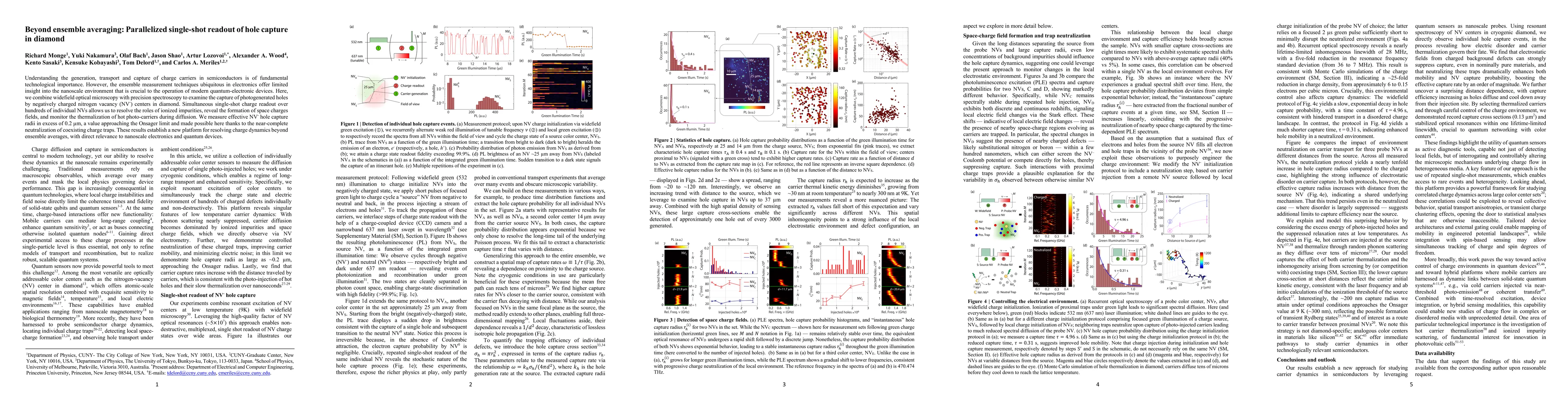
Understanding the generation, transport and capture of charge carriers in semiconductors is of fundamental technological importance. However, the ensemble measurement techniques ubiquitous in electronics offer limited insight into the nanoscale environment that is crucial to the operation of modern quantum-electronic devices. Here, we combine widefield optical microscopy with precision spectroscopy to examine the capture of photogenerated holes by negatively charged nitrogen vacancy (NV-) centers in diamond. Simultaneous single-shot charge readout over hundreds of individual NVs allows us to resolve the roles of ionized impurities, reveal the formation of space charges fields, and monitor the thermalization of hot photo-carriers during diffusion. We measure effective NV- hole capture radii in excess of 0.2 um, a value approaching the Onsager limit and made possible here thanks to the near-complete neutralization of coexisting charge traps. These results establish a new platform for resolving charge dynamics beyond ensemble averages, with direct relevance to nanoscale electronics and quantum devices.

AI Key Findings

Generated Sep 07, 2025

Methodology

The research combines widefield optical microscopy with precision spectroscopy to study the capture of photogenerated holes by negatively charged nitrogen vacancy (NV-) centers in diamond, utilizing simultaneous single-shot charge readout over hundreds of individual NVs.

Key Results

  • Effective NV- hole capture radii exceed 0.2 um, approaching the Onsager limit due to near-complete neutralization of coexisting charge traps.
  • Resolved roles of ionized impurities, formation of space charge fields, and monitored thermalization of hot photo-carriers during diffusion.
  • Established a new platform for resolving charge dynamics beyond ensemble averages, with direct relevance to nanoscale electronics and quantum devices.

Significance

This work provides insights into charge carrier dynamics at the nanoscale, crucial for understanding and advancing modern quantum-electronic devices.

Technical Contribution

The development of a widefield resonant imaging protocol for capturing PLE spectra across many individual NV centers in parallel, enabling simultaneous single-shot charge readout.

Novelty

This research presents a novel approach to studying charge carrier dynamics by leveraging the unique properties of NV centers in diamond, surpassing traditional ensemble measurement techniques.

Limitations

  • The study was conducted at a temperature of 9 K, which may limit direct applicability to room-temperature conditions.
  • The research focused on diamond samples with nitrogen doping, so findings might not generalize to other semiconductor materials.

Future Work

  • Investigate charge dynamics at room temperature to enhance practical applicability.
  • Explore the behavior in various other semiconductor materials to broaden the scope of the findings.

Paper Details

PDF Preview

Download PDF

Citation Network

Current paper (gray), citations (green), references (blue)

Display is limited for performance on very large graphs.

Current Paper
Citations
References
Click to view
Title Authors Year Actions

Comments (0)

This website uses cookies to ensure you get the best experience. Learn more