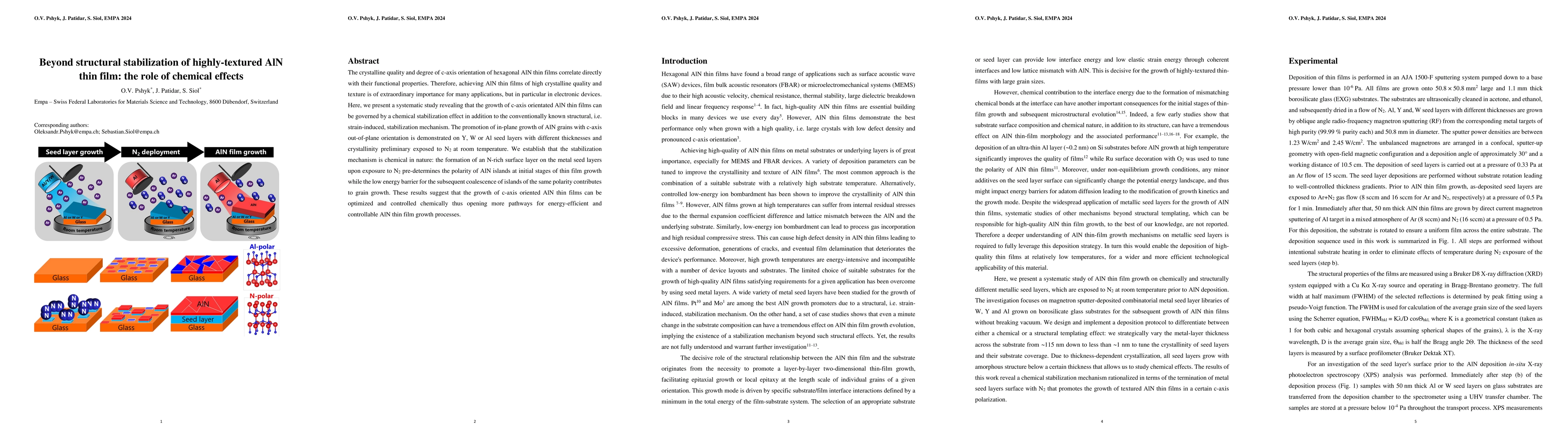
Improving the crystallinity and texture of oblique-angle-deposited AlN thin films using reactive synchronized HiPIMS
|
Jyotish Patidar, A. Sharma, S. Zhuk, G. Lorenzin, C. Cancellieri, Martin F. Sarott, M. Trassin, K. Thorwarth, J. Michler, Sebastian Siol Empa - Swiss Federal Laboratories for Materia Science, Coating Technologies, Empa - Swiss Federal Laboratories for Materials Science, Technology, Switzerland., Laboratory for Mechanics of Materials, Nanostructures, Laboratory for Joining Technologies, Corrosion, Department of Materials, Eth Zurich
|
2023
|
View Paper
|
Epitaxial Junction of Inversion Symmetry Breaking AlN and Centrosymmetric NbN: A Polarity Control of Wide-Bandgap AlN
|
A. Kobayashi, Shunya Kihira, T. Akiyama, T. Kawamura, T. Maeda, K. Ueno, H. Fujioka
|
2023
|
View Paper
|
Resolving Oxidation States and X–site Composition of Sn Perovskites through Auger Parameter Analysis in XPS
|
Alexander Wieczorek, Huagui Lai, Johnpaul K. Pious, F. Fu, S. Siol
|
2022
|
View Paper
|
Sputter Epitaxy of AlN and GaN on Si(111)
|
A. Dadgar, F. Hörich, Ralf Borgmann, J. Bläsing, G. Schmidt, P. Veit, J. Christen, A. Strittmatter
|
2022
|
View Paper
|
Molecular beam homoepitaxy of N-polar AlN: Enabling role of aluminum-assisted surface cleaning
|
Zexuan Zhang, Y. Hayashi, T. Tohei, A. Sakai, V. Protasenko, J. Singhal, H. Miyake, H. Xing, D. Jena, Y. Cho
|
2022
|
View Paper
|
Chemical state analysis of reactively sputtered zinc vanadium nitride: The Auger parameter as a tool in materials design
|
S. Zhuk, Sebastian Siol Empa - Swiss Federal Laboratories for Materia Science, Technology
|
2022
|
View Paper
|
Demonstration of lateral epitaxial growth of AlN on Si (1 1 1) at low temperatures by pulsed reactive sputter epitaxy
|
F. Hörich, Ralf Borgmann, J. Bläsing, G. Schmidt, P. Veit, F. Bertram, J. Christen, A. Strittmatter, A. Dadgar
|
2021
|
View Paper
|
Reduction of threading dislocation densities of N-polar face-to-face annealed sputtered AlN on sapphire
|
K. Shojiki, K. Uesugi, S. Kuboya, H. Miyake
|
2021
|
View Paper
|
Concepts for chemical state analysis at constant probing depth by lab‐based XPS/HAXPES combining soft and hard X‐ray sources
|
S. Siol, J. Mann, J. Newman, T. Miyayama, Katsumi Watanabe, P. Schmutz, C. Cancellieri, L. Jeurgens
|
2020
|
View Paper
|
Tunable ion flux density and its impact on AlN thin films deposited in a confocal DC magnetron sputtering system
|
M. Trant, M. Fischer, K. Thorwarth, S. Gauter, J. Patscheider, H. Hug
|
2018
|
View Paper
|
Stabilization of wide band-gap p-type wurtzite MnTe thin films on amorphous substrates
|
S. Siol, Yanbing Han, J. Mangum, P. Schulz, A. Holder, Talysa R Klein, Maikel F. A. M. Hest, B. Gorman, A. Zakutayev
|
2018
|
View Paper
|
AlN/nitrided sapphire and AlN/non-nitrided sapphire hetero-structures epitaxially grown by pulsed laser deposition: A comparative study
|
Jianghua Luo, Wenliang Wang, Yulin Zheng, Xiaochan Li, Guoqiang Li
|
2017
|
View Paper
|
Advances in piezoelectric thin films for acoustic biosensors, acoustofluidics and lab-on-chip applications
|
Y. Fu, Jack K. Luo, N. Nguyen, A. Walton, A. Flewitt, X. Zu, Yifan Li, G. McHale, A. Matthews, E. Iborra, H. Du, W. Milne
|
2017
|
View Paper
|
Core-level spectra and binding energies of transition metal nitrides by non-destructive x-ray photoelectron spectroscopy through capping layers
|
G. Greczynski, D. Primetzhofer, Jun Lu, L. Hultman
|
2017
|
View Paper
|
AlN films deposited by dc magnetron sputtering and high power impulse magnetron sputtering for SAW applications
|
K. A. Aissa, Amine Achour, Omar Elmazria, Quentin Simon, M. Elhosni, Pascal Boulet, S. Robert, M. Djouadi
|
2015
|
View Paper
|
Recommended Auger parameters for 42 elemental solids
|
C. Powell
|
2012
|
View Paper
|
Charge referencing issues in XPS of insulators as evidenced in the case of Al‐Si‐N thin films
|
A. Pélisson-Schecker, H. Hug, J. Patscheider
|
2012
|
View Paper
|
Calculations of electron inelastic mean free paths. IX. Data for 41 elemental solids over the 50 eV to 30 keV range
|
S. Tanuma, C. Powell, D. R. Penn
|
2011
|
View Paper
|
Sputtering of (001)AlN thin films: Control of polarity by a seed layer
|
E. Milyutin, S. Harada, D. Martin, J. Carlin, N. Grandjean, V. Savu, O. Vaszquez-Mena, J. Brugger, P. Muralt
|
2010
|
View Paper
|
Piezoelectric nanoelectromechanical resonators based on aluminum nitride thin films
|
R. Karabalin, M. Matheny, Xiaohua Feng, E. Defay, G. Rhun, C. Marcoux, S. Hentz, P. Andreucci, M. Roukes
|
2009
|
View Paper
|
Piezoelectric aluminum nitride nanoelectromechanical actuators
|
N. Sinha, G. E. Wabiszewski, R. Mahameed, V. Felmetsger, S. Tanner, R. Carpick, G. Piazza
|
2009
|
View Paper
|
Comparative study of c-axis AlN films sputtered on metallic surfaces
|
A. Sanz-Hervás, L. Vergara, J. Olivares, E. Iborra, Y. Morilla, J. Garcia-Lopez, M. Clement, J. Sangrador, M. A. Respaldiza
|
2005
|
View Paper
|
Summary of ISO/TC 201 Standard: VII ISO 15472 : 2001—surface chemical analysis—x‐ray photoelectron spectrometers—calibration of energy scales
|
M. Seah
|
2001
|
View Paper
|
Stress and piezoelectric properties of aluminum nitride thin films deposited onto metal electrodes by pulsed direct current reactive sputtering
|
M. Dubois, P. Muralt
|
2001
|
View Paper
|
Effect of substrate composition on the piezoelectric response of reactively sputtered AlN thin films
|
J. A. Ruffner, P. Clem, B. Tuttle, D. Dimos, D. Gonzales
|
1999
|
View Paper
|
High-quality AlN grown on Si(111) by gas-source molecular-beam epitaxy with ammonia
|
S. Nikishin, V. G. Antipov, S. Francoeur, N. Faleev, G. Seryogin, V. Elyukhin, H. Temkin, T. Prokofyeva, M. Holtz, A. Konkar, S. Zollner
|
1999
|
View Paper
|
Properties of aluminum nitride thin films for piezoelectric transducers and microwave filter applications
|
M. Dubois, P. Muralt
|
1999
|
View Paper
|
Control of preferential orientation of AlN films prepared by the reactive sputtering method
|
M. Ishihara, Songbin Li, H. Yumoto, K. Akashi, Y. Ide
|
1998
|
View Paper
|
Initial and final state effects in the ESCA spectra of cadmium and silver oxides
|
S. Gaarenstroom, N. Winograd
|
1977
|
View Paper
|
Influence of chemical interaction at the lattice-mismatched h-BN/Pt (111) interfaces on the overlayer morphology
|
|
2007
|
|
Thin Film Piezoelectrics for MEMS
|
S. Trolier-McKinstry, P. Muralt
|
2004
|
View Paper
|
Nature of nitrogen adsorbed on transition metal surfaces as revealed by electron spectroscopy and cognate techniques
|
C. Rao, G. Rao
|
1991
|
View Paper
|
XPS, UPS AND XAES studies of the adsorption of nitrogen, oxygen, and nitrogen oxides on W(110) at 300 and 100 K. II. Adsorption of NO
|
R. Masel, E. Umbach, J. Fuggle, D. Menzel
|
1979
|
View Paper
|
Chemical shifts of Auger lines, and the Auger parameter
|
C. D. Wagner
|
1975
|
View Paper
|
Comments (0)