ArxivLens

Quick Summary:

The paper proposes a novel lateral Bipolar Charge Plasma Transistor (BCPT) using 2-D simulations to induce n- and p-type charge layers on undoped SOI. Simulations show BCPTs achieving higher current gain compared to conventional BJTs, offering benefits for ultra-thin SOI structures by addressing doping challenges.

Journal Reference: IEEE Trans. on Electron Devices, Vol.59, pp:962-967, April 2012
arXiv Id: 1203.5670
Date Published: 2012-03-27
Date Updated: 2012-03-27

Categories:

Key Terms (TF-IDF):

lateral (0.360)
plasma (0.226)
issues (0.211)
concept (0.205)
charge (0.193)
electrodes (0.175)
junction (0.165)
doping (0.164)
activation (0.159)
doped (0.153)
compared (0.153)
electrical (0.152)
realize (0.150)
identical (0.149)
induce (0.148)
ultra (0.141)
results demonstrate (0.141)
simulation results (0.141)
device (0.139)
forming (0.139)
License: http://arxiv.org/licenses/nonexclusive-distrib/1.0/

Summary:

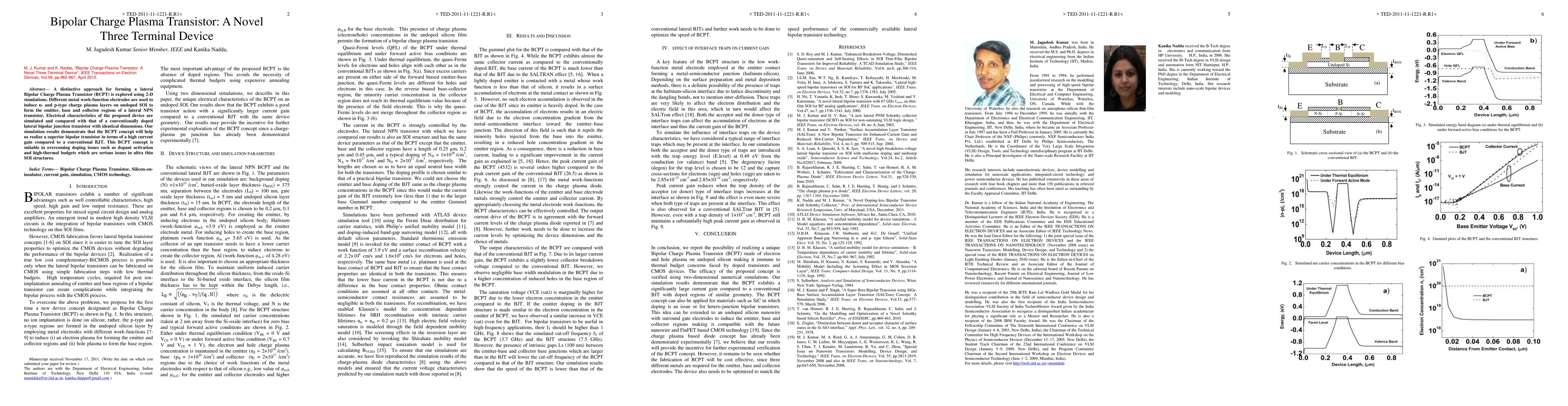
A distinctive approach for forming a lateral Bipolar Charge Plasma Transistor (BCPT) is explored using 2-D simulations. Different metal work-function electrodes are used to induce n- and p-type charge plasma layers on undoped SOI to form the emitter, base and collector regions of a lateral NPN transistor. Electrical characteristics of the proposed device are simulated and compared with that of a conventionally doped lateral bipolar junction transistor with identical dimensions. Our simulation results demonstrate that the BCPT concept will help us realize a superior bipolar transistor in terms of a high current gain compared to a conventional BJT. This BCPT concept is suitable in overcoming doping issues such as dopant activation and high-thermal budgets which are serious issues in ultra thin SOI structures.

Citation & Reference Network Visualization

This graph shows how this paper is connected to other research. The current paper is shown in dark gray, papers that cite it are in green, and papers it references are in blue. You can:

Current Paper
Papers citing this work (Citations)
Papers cited by this work (References)

• Hover over any node to see the paper title

• Click a node to view that paper's details

• Drag nodes to rearrange the graph

• Use the zoom controls (bottom right) to zoom in/out

Citations and References

Title Authors Year Actions
Improvement of digital, analog/RF and linearity performances of charge plasma based junctionless FinFET through spacer layer engineering
K. Banerjee, Abhijit Biswas
2024
View Paper
A Novel Fin-Shape Double-Gate GaAs p-MOSFET With Intrinsic Source and Enhanced Switching Performance
Iman Chahardah Cherik, Saeed Mohammadi
2024
View Paper
Design and reliability assessment of an ultra-thin body electrostatically doped bipolar transistor for mixed signal applications
Abhishek Sahu, Abhishek Kumar, Anurag Dwivedi, S. P. Tiwari
2024
View Paper
Doping-Less Feedback Field-Effect Transistors
Hakin Kim, Doohyeok Lim
2024
View Paper
Examination of Interface Trap Charges on Electrically Doped Tunnel FET in the Presence of High-K Dielectric
Student Member Ieee Bandi Venkata Chandan, Penjerla Srinivasa, Subbarao, Kaushal Kumar, Member Ieee Nigam
2023
View Paper
Doping-less MultiGate Inverted-T shape FET device with Schottky source/drain contacts
Sameeksha Munjal, Neelam Rup Prakash, Jasbir Kaur, Komal
2023
View Paper
Design and Analysis of the Electrical Properties of Different Dielectric Oxide Materials for Electrostatic Doping Through Nanowire Multichannel FET
R. S. Kumar, R. Ramya, S. A. Kumar
2023
View Paper
Charge-plasma-based inverted T-shaped source-metal dual-line tunneling FET with improved performance at 0.5 V operation
Aadil Anam, S. Amin, D. Prasad, Naveen Kumar, S. Anand
2023
View Paper
Comparative analysis of gate-oxide engineering in charge plasma based nanowire transistor
Joyprokash Debnath, Md Ezazul Haque Sikder, Showmik Singha
2023
View Paper
Design and Investigation of SRAM using Charge Plasma Dopingless Nanowire FET
Prateek Goel, Madan Gopal Agrawal, S. Anand, Pradeep Kumar, Leo Raj Solay
2023
View Paper
Design and simulation of junctionless nanowire tunnel field effect transistor for highly sensitive biosensor
Parveen Kumar, B. Raj
2023
View Paper
A high-performance doping-less tunnel FET with pocketed architecture: proposal and analysis
Nazia Haneef, M. A. Raushan, MD. Yasir Bashir, M. J. Siddiqui
2023
View Paper
Performance investigation of an InAs-based dielectric-modulated heterojunction TFET as a label-free biosensor
Swati, J. Kaur, Abdesh Kumar Singh
2023
View Paper
Enhanced analog/RF performance of hybrid charge plasma based junctionless C-FinFET amplifiers at 10 nm technology node
K. Banerjee, A. Biswas
2022
View Paper
Charge-plasma based symmetrical-gate complementary electron–hole bilayer TFET with improved performance for sub-0.5 V operation
Aadil Anam, Naveen Kumar, S. Amin, D. Prasad, S. Anand
2022
View Paper
Implementation of charge plasma based dopingless multi bridge channel MOSFET for enhanced performances
S. A. Kumar, J. Pravin, V. Sandeep, R. Sridevi
2022
View Paper
Physical Insight into electrostatically doped TFET considering Ambipolarity conduction
Nazia Haneef, MD. Yasir Bashir, M. A. Raushan, M. J. Siddiqui
2022
View Paper
Simulation Study of Charge Plasma Nanotube FET for Low Power Mixed Signal Circuit in IoT Applications
Rakesh Kumar, Pothaknuri Manasa, Ashutosh Srivastava
2022
View Paper
Design and Analysis of Charge Plasma Junction Less TFET Biosensing Applications
D. Manasawi, K. Srinivasa Rao
2022
View Paper
Design and performance augmentation of charge-plasma nanoFET with parametric analysis using non-equilibrium Green's function
Jainandan Kumar Modi, A. Raman, Prateek Kumar, Ravi Ranjan, Naveen Kumar
2022
View Paper
Performance Assessment and Optimization of Vertical Nanowire TFET for Biosensor Application
Parveen Kumar, B. Raj
2022
View Paper
Ohmic Junction Based Tunnel FET for High Frequency and Low Power Applications
Shivendra Yadav, Bhaskar Awadhiya, A. Mittal
2022
View Paper
Realization of Boolean Functions Using Heterojunction Tunnel FETs
V. Ambekar, Meena Panchore
2022
View Paper
Design and analysis of dopingless 1T DRAM using work function engineered tunnel field effect transistors
A. Arun, P. Sreelekshmi, Jobymol Jacob
2022
View Paper
Heterogenous Gate Dielectric DLTFET: Reliability Perspective Against Degradation Mechanisms
Kanchan Cecil, Meena Panchore, D. P. Samajdar
2021
View Paper
Investigation of Charge-plasma Based Dopingless Tunnel FET for Analog/RF and Linear Applications
Suruchi Sharma, R. Basu, B. Kaur
2021
View Paper
Terahertz radiation from silicon carbide charge plasma avalanche transit time source
A. Acharyya
2021
View Paper
Parametric Investigation and Design of Junctionless Nanowire Tunnel Field Effect Transistor
Parveen Kumar, B. Raj
2021
View Paper
Ultra Steep Ge-Source Dopingless Tunnelling Field Effect Transistor with Enhanced Drive Current: DC to Linearity Characteristics Analysis
Kumari Nibha Priyadarshani, Sangeeta Singh, Kunal Singh
2021
View Paper
Parameter Variation Analysis of Dopingless and Junctionless Nanotube MOSFET
S. Bala, Raj Kumar, Arvind Kumar
2021
View Paper
Comparative study of doped and doping less charge plasma silicon microstrip detector
Rakesh Kumar, Jitendra Kumar, L. Beloni Devi, Kundan Singh
2021
View Paper
Capacitive Analysis of Strained Superjunction Vertical Single Diffused MOSFET
Onika Parmar, Payal Nautiyal, Alok Naugarhiya
2021
View Paper
Insights into temperature influence on analog/RF and linearity performance of a Si/Ge heterojunction asymmetric double gate dopingless TFET
Suruchi Sharma, R. Basu, B. Kaur
2021
View Paper
Insights into temperature influence on analog/RF and linearity performance of a Si/Ge heterojunction asymmetric double gate dopingless TFET
Suruchi Sharma, R. Basu, B. Kaur
2021
View Paper
Modeling and Simulation-Based Investigation of 2-D Symmetric Double Gate Dopingless-TFET and Its Circuit Performance for Low-Power Applications
Monika Sharma, R. Narang, M. Saxena, Mridula Gupta
2021
View Paper
Ground Plane Electrostatically Doped Junctionless Tunnel Field Effect Transistor: Process Immune Design for Suppressed Ambipolarity
Aishwarya Kaity, Sangeeta Singh, K. K. Jha
2021
View Paper
Design and Analysis of Gate Engineered Gate-AII-Around (GAA) Charge Plasma Nanowire Field Effect Transistor
Leo Raj Solay, Pradeep Kumar, Intekhab Amin, S. Anand
2021
View Paper
Non-Destructive Label-Free Biomaterials Detection Using Tunneling Carbon Nanotube-Based Biosensor
M. Ghodrati, A. Mir, A. Farmani
2021
View Paper
Exploration of logic gates and multiplexer using doping-free bipolar junction transistor
A. Sahu, Abhishek Kumar, S. P. Tiwari
2021
View Paper
Interface trap charges associated reliability analysis of Si/Ge heterojunction dopingless TFET
Suruchi Sharma, R. Basu, B. Kaur
2021
View Paper
Impact of Work Function Engineering in Charge Plasma Based Bipolar Devices
L. Bramhane, S. Salankar, Mahendra U. Gaikwad, Meena Panchore
2021
View Paper
Implementation of Boolean Functions Using Tunnel Field-Effect Transistors
S. Garg, Sneh Saurabh
2020
View Paper
A Novel Self-Aligned Dopingless Symmetric Tunnel Field Effect Transistor (DL-STFET): A Process Variations Tolerant Design
Kumari Nibha Priyadarshani, Sangeeta Singh, Kunal Singh
2020
View Paper
Design and optimization of junctionless-based devices with noise reduction for ultra-high frequency applications
Krishan Kumar, A. Raman, B. Raj, Sarabdeep Singh, Naveen Kumar
2020
View Paper
Virtually Doped Silicon-on-Insulator Junctionless Transistor for Reduced OFF-State Leakage Current
Prateek Kishor Verma, S. Gupta
2020
View Paper
Contact engineered charge plasma junctionless transistor for suppressing tunneling leakage
Harendra Kumar, Sangeeta Singh, Kumari Nibha Priyadarshani, J. Ghosh, Alok Naugarhiya
2020
View Paper
Metal controlled nanoscaled dopingless MOSFET on selective/partial buried oxide
F. Bashir, Asim M. Murshid, S. Loan
2020
View Paper
Realizing XOR and XNOR Functions Using Tunnel Field-Effect Transistors
S. Garg, Sneh Saurabh
2020
View Paper
Improved digital performance of charge plasma based junctionless C-FinFETs at 10 nm technology node and beyond
K. Banerjee, A. Biswas
2020
View Paper
A Comprehensive Review on Tunnel Field-Effect Transistor (TFET) Based Biosensors: Recent Advances and Future Prospects on Device Structure and Sensitivity
N. Reddy, D. Panda
2020
View Paper
Investigation of Pd/MoOx/n-Si diodes for bipolar transistor and light-emitting device applications
G. Gupta, Shivakumar D. Thammaiah, L. Nanver, R. Hueting
2020
View Paper
Electrothermal analysis of novel N-P-P FinFET with electrically doped drain: a dual material gate device for reliable nanoscale applications
F. Karimi, Z. Ramezani, I. Amiri, Alireza Mahdavi Nejad
2020
View Paper
Electrothermal analysis of novel N-P-P FinFET with electrically doped drain: a dual material gate device for reliable nanoscale applications
F. Karimi, Z. Ramezani, I. S. Amiri, Alireza Mahdavi Nejad
2020
View Paper
Performance Analysis of Channel and Inner Gate Engineered GAA Nanowire FET
Ashima, D. Vaithiyanathan, B. Raj
2020
View Paper
Design and Analysis of Double Gate Tunnel Field Effect Transistor using Charged Plasma
Hemanga Banerjee, K. Sarkar, Papiya Debnath, Swarnil Roy, M. Chanda
2020
View Paper
Detection of Biomolecules Using Charge-Plasma Based Gate Underlap Dielectric Modulated Dopingless TFET
S. K. Verma, Shailendra Singh, Girish Wadhwa, B. Raj
2020
View Paper
A charge-plasma-based dual-metal-gate recessed-source/drain dopingless junctionless transistor with enhanced analog and RF performance
Prateek Kishor Verma, Y. Verma, Varun Mishra, Santosh Kumar Gupta
2020
View Paper
A charge-plasma-based dual-metal-gate recessed-source/drain dopingless junctionless transistor with enhanced analog and RF performance
Prateek Kishor Verma, Y. Verma, Varun Mishra, Santosh Kumar Gupta
2020
View Paper
GaAs0.5Sb0.5/ In0.53Ga0.47As heterojunction dopingless charge plasma-based tunnel FET for analog/digital performance improvement
Amit Bhattacharyya, M. Chanda, D. De
2020
View Paper
Charge-Plasma-Based Negative Capacitance Ring-FET: Design, Investigation and Reliability Analysis
A. K. Gupta, A. Raman, Naveen Kumar
2020
View Paper
Low voltage charge-plasma based dopingless Tunnel Field Effect Transistor: analysis and optimization
Naveen Kumar, A. Raman
2020
View Paper
Silicon-On-Nothing Electrostatically Doped Junctionless Tunnel Field Effect Transistor (SON-ED-JLTFET): A Short Channel Effect Resilient Design
Aishwarya Kaity, Sangeeta Singh, Pravin N. Kondekar
2020
View Paper
Proposal of Charge Plasma Based Recessed Source/Drain Dopingless Junctionless Transistor and its Linearity Distortion Analysis for Circuit Applications
Prateek Kishor Verma, S. Gupta
2020
View Paper
Design and Investigation of Pressure Sensor Based on Charge Plasma Silicon NWFET with Cylindrical Gate Diaphragm
Sarabdeep Singh, A. Raman
2020
View Paper
Design and Analog Performance Analysis of Charge-Plasma Based Cylindrical GAA Silicon Nanowire Tunnel Field Effect Transistor
Naveen Kumar, A. Raman
2019
View Paper
Hetero-Dielectric oxide engineering on dopingless gate all around nanowire MOSFET with Schottky contact source/drain
Agamreet Kaur, R. Mehra, Amit Saini
2019
View Paper
A Nano junctionless Double-Gate MOSFET by Using the Charge Plasma Concept to Improve Short-Channel Effects and Frequency Characteristics
Z. Ramezani, A. Orouji, S. A. Ghoreishi, I. Amiri
2019
View Paper
Low voltage charge-plasma based dopingless Tunnel Field Effect Transistor: analysis and optimization
Naveen Kumar, A. Raman
2019
View Paper
Design and Simulation of High Performance Dopingless Tunnel Diode
F. Bashir, Asim Majeed, F. A. Khanday, M. T. Banday
2019
View Paper
A novel Ge based overlapping gate dopingless tunnel FET with high performance
Shupeng Chen, Hongxia Liu, Shulong Wang, Tao Han, Wei Li, Xing Wang
2019
View Paper
Comparative study of InGaN and InGaAs based dopingless TFET with different gate engineering techniques
Monika Sharma, R. Narang, M. Saxena, Mridula Gupta
2019
View Paper
A fair comparison of the performance of charge plasma and electrostatic tunnel FETs for low-power high-frequency applications
Bandi Venkata Chandan, K. Nigam, Chithraja Rajan, D. Sharma
2019
View Paper
A better TID hardened Dopingless Lateral Bipolar Transitor on SiGe-OI design
L. B. Devi, Jitendra Kumar, A. Srivastava
2019
View Paper
Dopingless 1T DRAM: Proposal, Design, and Analysis
A. James, Sneh Saurabh
2019
View Paper
A novel design approach of charge plasma tunnel FET for radio frequency applications
Shivendra Yadav, Alish Pamnani, D. Sharma, Anju Gedam, Atul Kumar, Neeraj Sharma
2019
View Paper
Triple-sided charged plasma symmetric lateral bipolar transistor on SiGe-OI
L. B. Devi, Kundan Singh, Jitendra Kumar, A. Srivastava
2019
View Paper
Performance Improvement and Analysis of PtSi Schottky Barrier p-MOSFET Based on Charge Plasma Concept for Low Power Applications
S. Kale
2019
View Paper
Junction-less optical phase shifter loaded silicon Mach–Zehnder modulator
Subhradeep Pal, Sumanta Gupta
2019
View Paper
Comparative Study of Different Configurations in Triple-Sided Charged Plasma Symmetric Lateral Heterojunction Bipolar Transistors on SOI
L. Beloni Devi, A. Srivastava
2019
View Paper
Approach on electrically doped TFET for suppression of ambipolar and improving RF performance
Bandi Venkata Chandan, K. Nigam, D. Sharma
2019
View Paper
Design and Analysis of Novel Charge-Plasma Based Dopingless U-Shaped FET
Naveen Kumar, A. Raman
2019
View Paper
An Effective Charge Plasma based Semi-Superjunction MOSFET
Ajeet Singh Lowanshi, Onika Parmar, Anshul Gupta, Alok Naugarhiya
2019
View Paper
Tunnel Field Effect Transistor for Ultra Low Power Applications: A Review
Km. Sucheta Singh, Satyendra Kumar, K. Nigam, V. Tikkiwal
2019
View Paper
Design and analysis of dynamically configurable electrostatic doped carbon nanotube tunnel FET
Amandeep Singh, Mamta Khosla, B. Raj
2019
View Paper
Junctionless Devices Without Any Chemical Doping
2019
View Paper
A computational study of a carbon nanotube junctionless tunneling field-effect transistor (CNT-JLTFET) based on the charge plasma concept
Seyyedeh Hoda Tahaei, Seyed Saleh Ghoreishi, R. Yousefi, Habib Aderang
2019
View Paper
Electrostatically Doped DSL Schottky Barrier MOSFET on SOI for Low Power Applications
F. Bashir, Abdullah G. Alharbi, S. Loan
2018
View Paper
Impact of gate material engineering on ED‐TFET for improving DC/analogue‐RF/linearity performances
Bandi Venkata Chandan, Sushmitha Dasari, K. Nigam, Shivendra Yadav, S. Pandey, D. Sharma
2018
View Paper
Design and analysis of electrostatic doped tunnel CNTFET for various process parameters variation
S. Bala, Mamta Khosla
2018
View Paper
Impact of strained silicon on the device performance of a bipolar charge plasma transistor
Sangeeta Singh
2018
View Paper
Device and circuit level performance assessment of n‐ and p‐type dopingless MOSFETs
F. Bashir, Asim M. Murshid, M. T. Banday
2018
View Paper
Effective approach to enhance DC and high‐frequency performance of electrically doped TFET
Shivendra Yadav, Alemienla Lemtur, D. Sharma, M. Aslam, Deepak Soni
2018
View Paper
Electrostatically doped tunnel CNTFET model for low-power VLSI circuit design
S. Bala, Mamta Khosla
2018
View Paper
Low Power and Low Area Junction-less Tunnel FET Design
U. Ragavendran, M. Ramachandran
2018
View Paper
Parametric Variation Analysis of Symmetric Double Gate Charge Plasma JLTFET for Biosensor Application
Girish Wadhwa, B. Raj
2018
View Paper
Gate-All-Around Charge Plasma-Based Dual Material Gate-Stack Nanowire FET for Enhanced Analog Performance
Sarabdeep Singh, A. Raman
2018
View Paper
Impact of interface trap charges on dopingless tunnel FET for enhancement of linearity characteristics
Bandi Venkata Chandan, K. Nigam, D. Sharma, S. Pandey
2018
View Paper
Impact of interface trap charges on dopingless tunnel FET for enhancement of linearity characteristics
Bandi Venkata Chandan, K. Nigam, D. Sharma, S. Pandey
2018
View Paper
Incorporation of hafnium and platinum metal in vertical power MOSFETs
Onika Parmar, Alok Naugarhiya
2018
View Paper
Charge Plasma High Voltage PIN Diode Investigation
M. J. Kumar, Sara Hahmady, R. Gale, S. Bayne
2018
View Paper
Analysis and modeling of unipolar junction transistor with excellent performance: a novel DG MOSFET with $${N}^{+}{-}{P}^{-}$$N+-P- junction
Z. Ramezani, A. Orouji
2018
View Paper
Label Free Detection of Biomolecules Using Charge-Plasma-Based Gate Underlap Dielectric Modulated Junctionless TFET
Girish Wadhwa, B. Raj
2018
View Paper
Source/Drain Engineered Charge-Plasma Junctionless Transistor for the Immune of Line Edge Roughness Effect
Wenbo Wan, H. Lou, Ying Xiao, Xinnan Lin
2018
View Paper
Approach to suppress ambipolarity and improve RF and linearity performances on ED‐Tunnel FET
Bandi Venkata Chandan, Sushmitha Dasari, Shivendra Yadav, D. Sharma
2018
View Paper
A dopingless gate-all-around (GAA) gate-stacked nanowire FET with reduced parametric fluctuation effects
Sarabdeep Singh, A. Raman
2018
View Paper
A dopingless gate-all-around (GAA) gate-stacked nanowire FET with reduced parametric fluctuation effects
Sarabdeep Singh, A. Raman
2018
View Paper
Design and performance projection of workfunction engineered variable vertical doped superjunction vertical single diffused MOS
Payal Nautiyal, Onika Parmar, Alok Naugarhiya, Shrish Verma
2018
View Paper
Design and simulation of a doping-less charge plasma based enhancement mode GaN MOSFET
S. Verma, S. Loan, A. Alamoud
2018
View Paper
Application of Workfunction Engineering in Lateral Power Devices
Onika Parmar, Alok Naugarhiya
2018
View Paper
Charge Plasma Based VVD-SJ VDMOS Employing Reversed Doping Concentration
Payal Nautiyal, Alok Naugarhiya, Shrish Verma
2018
View Paper
Hybrid AlGaN/GaN high-electron mobility transistor: design and simulation
S. Verma, S. Loan, A. R. Alamoud, Abdullah G. Alharbi
2018
View Paper
A high-performance channel engineered charge-plasma-based MOSFET with high-κ spacer
Chan Shan, Ying Wang, Xin Luo, Mengtian Bao, Chenghao Yu, Fei Cao
2017
View Paper
Charge plasma based source/drain engineered Schottky Barrier MOSFET: Ambipolar suppression and improvement of the RF performance
S. Kale, P. Kondekar
2017
View Paper
Temperature sensitivity analysis on analog/RF and linearity metrics of electrically doped tunnel FET
Bandi Venkata Chandan, K. Nigam, S. Pandey, D. Sharma, P. Kondekar
2017
View Paper
Design and simulation of a doping-less charge plasma based enhancement mode GaN MOSFET
S. Verma, S. Loan, A. Alamoud
2017
View Paper
The concept of electrostatic doping and related devices
S. Cristoloveanu, K. Lee, Hyungjin Park, M. Parihar
2017
View Paper
Design and analysis of electrostatic doped Schottky barrier CNTFET based low power SRAM
Amandeep Singh, Mamta Khosla, B. Raj
2017
View Paper
Application of workfunction engineering in vertical superjunction devices
Payal Nautiyal, Alok Naugarhiya, Shrish Verma
2017
View Paper
Improved performance of impact ionization MOSFETs by using dopingless concept and strained channel
Mirgender Kumar, Si-Hyun Park
2017
View Paper
Charge plasma technique based dopingless accumulation mode junctionless cylindrical surrounding gate MOSFET: analog performance improvement
Nitin Trivedi, M. Kumar, S. Haldar, S. Deswal, Mridula Gupta, Rashmi Gupta
2017
View Paper
Charge plasma technique based dopingless accumulation mode junctionless cylindrical surrounding gate MOSFET: analog performance improvement
Nitin Trivedi, M. Kumar, S. Haldar, S. Deswal, Mridula Gupta, R. Gupta
2017
View Paper
Induced dielectric modulated tunnel field effect transistor biosensor (I-DMTFET): Proposal and investigation
Sumeet Kalra, M. J. Kumar, A. Dhawan
2017
View Paper
Electrostatic Doping in Semiconductor Devices
G. Gupta, B. Rajasekharan, R. Hueting
2017
View Paper
Controlling ambipolarity with improved RF performance by drain/gate work function engineering and using high $$\kappa $$κ dielectric material in electrically doped TFET: proposal and optimization
Shivendra Yadav, D. Sharma, Deepak Soni, M. Aslam
2017
View Paper
Potential benefits of graded channel dopingless transistor with source side dual-k spacer to upgrade analog/RF performance
P. Rani, S. Meena
2017
View Paper
A novel electrostatically doped ferroelectric Schottky barrier tunnel FET: process resilient design
Sangeeta Singh, P. Kondekar
2017
View Paper
A novel electrostatically doped ferroelectric Schottky barrier tunnel FET: process resilient design
Sangeeta Singh, P. Kondekar
2017
View Paper
Improved performance of bipolar charge plasma transistor by reducing the horizontal electric field
L. Bramhane, Jawar Singh
2017
View Paper
Tunneling Effects in a Charge-Plasma Dopingless Transistor
Jae Hur, Dong-il Moon, Jin-woo Han, Gun-Hee Kim, C. Jeon, Yang-Kyu Choi
2017
View Paper
Charge plasma based graded channel with dual material double gate JLT for enhance analog/RF performance
Amrish Kumar, Abhinav Gupta, Sanjeev Rai
2017
View Paper
Mixed-Mode Simulation of Common Emitter Amplifier Design Using Bipolar Charge Plasma Transistor
Chitrakant Sahu, Nitesh Agrawal
2016
View Paper
A novel gate and drain engineered charge plasma tunnel field-effect transistor for low sub-threshold swing and ambipolar nature
D. Yadav, Bhagwan Ram Raad, D. Sharma
2016
View Paper
Charge plasma based partial-ground-plane-MOSFET on selective buried oxide (SELBOX)
F. Bashir, S. Loan, Asim M. Murshid, A. Alamoud
2016
View Paper
Drain Work Function Engineered Doping-Less Charge Plasma TFET for Ambipolar Suppression and RF Performance Improvement: A Proposal, Design, and Investigation
Bhagwan Ram Raad, D. Sharma, P. Kondekar, K. Nigam, D. Yadav
2016
View Paper
The immunity of doping-less junctionless transistor variations including the line edge roughness
Wenbo Wan, H. Lou, Ying Xiao, Xinnan Lin
2016
View Paper
Study of DC and AC characteristics of gate-stack doping-less tunnel FET
Deepali Vasnik, M. Pattanaik
2016
View Paper
High frequency performance of dual metal gate vertical tunnel field effect transistor based on work function engineering
K. Nigam, P. Kondekar, D. Sharma
2016
View Paper
Symmetric Lateral Doping-Free BJT: A Novel Design for Mixed Signal Applications
A. Sahu, L. Bramhane, Jawar Singh
2016
View Paper
A Charge-Plasma-Based Transistor With Induced Graded Channel for Enhanced Analog Performance
Chan Shan, Ying Wang, Mengtian Bao
2016
View Paper
Junction and doping-free transistors for future computing
Chitrakant Sahu, Jawar Singh
2016
View Paper
TCAD simulation of germanium source dopingless tunnel FET
R. Juyal, S. S. Chauhan
2016
View Paper
Enhanced analog performance of doping-less dual material and gate stacked architecture of junctionless transistor with high-k spacer
S. Amin, R. Sarin
2016
View Paper
Enhanced analog performance of doping-less dual material and gate stacked architecture of junctionless transistor with high-k spacer
S. Amin, R. Sarin
2016
View Paper
Hetero Gate Material and Dual Oxide Dopingless Tunnel FET
Shuja A. Abbassi, F. Bashir, S. Loan, A. Alamoud, M. Nizamuddin, M. Rafat
2016
View Paper
Scalability and process induced variation analysis of polarity controlled silicon nanowire transistor
Chitrakant Sahu, Jawar Singh
2016
View Paper
Temperature sensitivity analysis of dopingless charge-plasma transistor
V. Shrivastava, Anup Kumar, Chitrakant Sahu, Jawar Singh
2016
View Paper
Performance analysis of charge plasma based dual electrode tunnel FET
S. Anand, S. Amin, R. Sarin
2016
View Paper
Transient performance estimation of charge plasma based negative capacitance junctionless tunnel FET
Sangeeta Singh, P. Kondekar, Pawan Pal
2016
View Paper
Performance Enhancement of Dopingless Tunnel-FET Based on Ge-Source with High-k
Kanchan Cecil, Jawar Singh
2015
View Paper
Extended Base Schottky-Collector Bipolar Charge Plasma Transistor
L. Bramhane, Jawar Singh
2015
View Paper
Charge-plasma based dual-material and gate-stacked architecture of junctionless transistor for enhanced analog performance
S. Amin, R. Sarin
2015
View Paper
Work function engineered charge plasma diodes for enhanced performance
Preeti Singh, S. Pandey
2015
View Paper
Investigation of laterally single-diffused metal oxide semiconductor (LSMOS) field effect transistor
Avikal Bansal, M. J. Kumar
2015
View Paper
PNPN tunnel FET with controllable drain side tunnel barrier width: Proposal and analysis
D. Abdi, M. J. Kumar
2015
View Paper
A High-Performance Source Engineered Charge Plasma-Based Schottky MOSFET on SOI
F. Bashir, S. Loan, M. Rafat, A. Alamoud, S. A. Abbasi
2015
View Paper
Reliability analysis of charge plasma based double material gate oxide (DMGO) SiGe-on-insulator (SGOI) MOSFET
K. P. Pradhan, P. K. Sahu, D. Singh, Laurent Artola, S. K. Mohapatra
2015
View Paper
Scalability and process induced variation analysis of polarity controlled silicon nanowire transistor
Chitrakant Sahu, Jawar Singh
2015
View Paper
GaAs Tunnel Diode With Electrostatically Doped n-Region: Proposal and Analysis
M. J. Kumar, S. Sharma
2015
View Paper
PVT-Aware Design of Dopingless Dynamically Configurable Tunnel FET
Avinash Lahgere, Chitrakant Sahu, Jawar Singh
2015
View Paper
Symmetric bipolar charge-plasma transistor with extruded base for enhanced performance
L. Bramhane, N. Upadhyay, J. R. Veluru, Jawar Singh
2015
View Paper
A high performance gate engineered charge plasma based tunnel field effect transistor
F. Bashir, S. Loan, M. Rafat, A. Alamoud, S. A. Abbasi
2015
View Paper
Dopingless PNPN tunnel FET with improved performance: Design and analysis
M. Ram, D. Abdi
2015
View Paper
Recent research trends in gate engineered tunnel FET for improved current behavior by subduing the ambipolar effects: A review
N. Bagga, S. Sarkhel, S. Sarkar
2015
View Paper
Junctionless Biristor: A Bistable Resistor Without Chemically Doped P-N Junctions
M. J. Kumar, M. Maheedhar, P. Varma
2015
View Paper
A Silicon Biristor With Reduced Operating Voltage: Proposal and Analysis
M. J. Kumar, M. Maheedhar, P. Varma
2015
View Paper
A high performance gate engineered charge plasma based tunnel field effect transistor
F. Bashir, S. Loan, M. Rafat, A. Alamoud, S. A. Abbasi
2015
View Paper
Potential Benefits and Sensitivity Analysis of Dopingless Transistor for Low Power Applications
Chitrakant Sahu, Jawar Singh
2015
View Paper
Dopingless impact ionization MOS (DL-IMOS)—a remedy for complex process flow
Sangeeta Singh, P. Kondekar
2015
View Paper
Vertical Bipolar Charge Plasma Transistor with Buried Metal Layer
K. Nadda, M. J. Kumar
2015
View Paper
Single Grain Boundary Dopingless PNPN Tunnel FET on Recrystallized Polysilicon: Proposal and Theoretical Analysis
M. Ram, D. Abdi
2015
View Paper
High performance charge plasma based multi zone lateral bipolar junction transistor
S. Loan, F. Bashir, M. Rafat, S. A. Abbasi, A. Alamoud
2014
View Paper
Dopingless tunnel FET with a hetero-material gate: Design and analysis
M. Ram, D. Abdi
2014
View Paper
Design and simulation of a high performance dopingless p-tunnel field effect transistor
F. Bashir, S. Loan
2014
View Paper
In-Built N+ Pocket p-n-p-n Tunnel Field-Effect Transistor
D. Abdi, M. J. Kumar
2014
View Paper
A high performance double gate dopingless metal oxide semiconductor field effect transistor
S. Loan, F. Bashir, M. Rafat, A. Alamoud, S. A. Abbasi
2014
View Paper
Junctionless Impact Ionization MOS: Proposal and Investigation
S. Ramaswamy, M. J. Kumar
2014
View Paper
Design and performance projection of symmetric bipolar charge-plasma transistor on SOI
Chitrakant Sahu, A. Ganguly, Jawar Singh
2014
View Paper
A high performance charge plasma PN-Schottky collector transistor on silicon-on-insulator
S. Loan, F. Bashir, M. Rafat, A. Alamoud, S. A. Abbasi
2014
View Paper
Dopingless super-steep impact ionisation MOS (dopingless-IMOS) based on workfunction engineering
S. Singh, P. Kondekar
2014
View Paper
Thin-Film Bipolar Transistors on Recrystallized Polycrystalline Silicon Without Impurity Doped Junctions: Proposal and Investigation
K. Nadda, M. J. Kumar
2014
View Paper
Charge-Plasma Based Process Variation Immune Junctionless Transistor
Chitrakant Sahu, Jawar Singh
2014
View Paper
Doping-Less Tunnel Field Effect Transistor: Design and Investigation
M. Jagadesh Kumar, S. Janardhanan
2013
View Paper
Schottky Collector Bipolar Transistor Without Impurity Doped Emitter and Base: Design and Performance
K. Nadda, M. J. Kumar
2013
View Paper
Doping-less Bipolar Transistor with fT Surpassing that of Conventional BJT
M. J. Kumar, K. Nadda
2013
View Paper
Performance Improvement in DRAM Cell Using Novel Nitride/Metal Spacers Structure
Seung-Geun Jung, Seong-Ji Min, Hyun-Yong Yu
2024
View Paper
Design and Parametric Analysis of Charge Plasma Junctionless TFET for Biosensor Applications
D. Manaswi, S. Karumuri, Girish Wadhwa
2023
View Paper
2-D Design of Double Gate Schottky Tunnel MOSFET for High-Performance Use in Analog/RF Applications
Shazia Rashid, F. Bashir, F. A. Khanday, M. R. Beigh, F. Hussin
2021
View Paper
Electrostatic doping and related devices
S. Cristoloveanu
2021
View Paper
Impact of Underlap/Overlap of Germanium Source Dopingless Tunnel Field Effect Transistor (Ge-S-DLTFET)
Kumari Nibha Priyadarshani, Sangeeta Singh
2021
View Paper
Doping-Less SiC p-i-n Diode: Design and Investigation
Sara Hahmady, S. Bayne
2021
View Paper
Reverse Recovery of 50 V Silicon Charge Plasma PIN Diode
Sara Hahmady, S. Bayne
2020
View Paper
The Charge Plasma n-p-n Impact Ionization MOS on FDSOI Technology: Proposal and Analysis
Avinash Lahgere, M. J. Kumar
2017
View Paper
Influence of Germanium source on dopingless tunnel-FET for improved analog/RF performance
Kanchan Cecil, Jawar Singh
2017
View Paper
Two-zone SiGe base heterojunction bipolar charge plasma transistor for next generation analog and RF applications
L. Bramhane, Jawar Singh
2017
View Paper
Silicon-Based Junctionless MOSFETs: Device Physics, Performance Boosters and Variations
Xinnan Lin, H. Lou, Ying Xiao, Wenbo Wan, Lining Zhang, M. Chan
2017
View Paper
Performance investigation of charge plasma based dual material gate junctionless transistor
S. Amin, S. Anand, R. Sarin
2016
View Paper
Charge Plasma Based Bipolar Junction Transistor on Silicon on Insulator
S. Loan, F. Bashir, Asim M. Murshid, Humyra Shabir, M. Rafat, M. Nizamuddin, A. R. Alamoud, S. A. Abbasi
2015
View Paper
A Novel High Performance Nanoscaled Dual Oxide Doping Less Tunnel Field Effect Transistor
S. Loan, F. Bashir, M. Rafat, M. Nizamuddin, Asim M. Murshid, Abdul, Rahman M. Alamoud, S. A. Abbasi
2014
View Paper
DESIGN AND ANALYSIS OF GATE-STACK DOPING-LESS TUNNEL FIELD EFFECT TRANSISTOR
Deepali Vasnik
2014
View Paper
A Novel High Performance Nanoscaled Dopingless Lateral PNP Transistor on Silicon on Insulator
F. Bashir, S. Loan, M. Nizamuddin, Humyra Shabir, M. Asim., Murshid, M. Rafat, A. R. Alamoud, S. A. Abbasi
2014
View Paper
A high performance charge plasma based lateral bipolar transistor on selective buried oxide
S. Loan, F. Bashir, M. Rafat, A. Alamoud, S. A. Abbasi
2013
View Paper
K. Nadda and M. J. Kumar, “Schottky Collector Bipolar Transistor without Impurity Doped Emitter and Base: Design
K. Nadda, M. J. Kumar, K. Nadda, M. J. Kumar
2013
View Paper

Comments (0)

This website uses cookies to ensure you get the best experience. Learn more