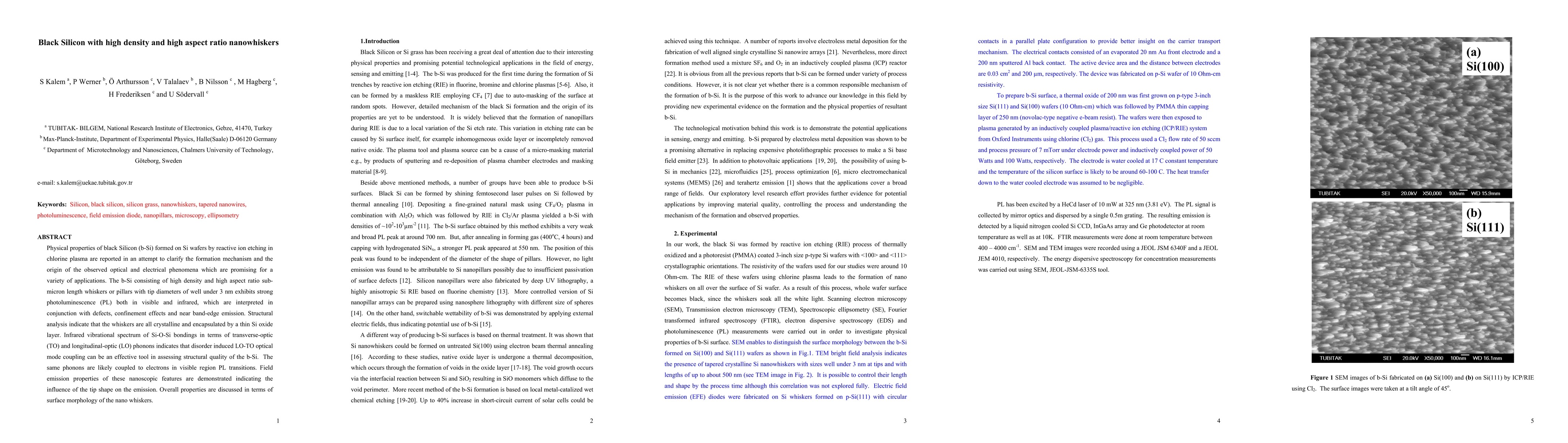
ArxivLens

Quick Summary:

This paper investigates the physical properties of black silicon formed via reactive ion etching, focusing on its high density and high aspect ratio nanowhiskers. The study reveals strong photoluminescence and field emission properties, attributing these phenomena to crystalline whiskers and their oxide layer, with implications for various applications.

Journal Reference: Nanotechnology 22 (2011) 235307
DOI: 10.1088/0957-4484/22/23/235307
arXiv Id: 1105.3011
Report No: 29ac
Date Published: 2011-05-17
Date Updated: 2011-05-17

Key Terms (TF-IDF):

si (0.339)
si (0.330)
pl (0.225)
tip (0.218)
tip (0.217)
phonons (0.209)
visible (0.190)
visible (0.181)
emission (0.172)
emission (0.169)
structural (0.165)
infrared (0.164)
infrared (0.161)
structural (0.159)
oxide (0.131)
optical (0.130)
micron (0.128)
optical (0.127)
high density (0.127)
physical properties (0.126)
License: http://arxiv.org/licenses/nonexclusive-distrib/1.0/

Summary:

Physical properties of black Silicon (b-Si) formed on Si wafers by reactive ion etching in chlorine plasma are reported in an attempt to clarify the formation mechanism and the origin of the observed optical and electrical phenomena which are promising for a variety of applications. The b-Si consisting of high density and high aspect ratio sub-micron length whiskers or pillars with tip diameters of well under 3 nm exhibits strong photoluminescence (PL) both in visible and infrared, which are interpreted in conjunction with defects, confinement effects and near band-edge emission. Structural analysis indicate that the whiskers are all crystalline and encapsulated by a thin Si oxide layer. Infrared vibrational spectrum of Si-O-Si bondings in terms of transverse-optic (TO) and longitudinal-optic (LO) phonons indicates that disorder induced LO-TO optical mode coupling can be an effective tool in assessing structural quality of the b-Si. The same phonons are likely coupled to electrons in visible region PL transitions. Field emission properties of these nanoscopic features are demonstrated indicating the influence of the tip shape on the emission. Overall properties are discussed in terms of surface morphology of the nano whiskers.

Citation & Reference Network Visualization

This graph shows how this paper is connected to other research. The current paper is shown in dark gray, papers that cite it are in green, and papers it references are in blue. You can:

Current Paper
Papers citing this work (Citations)
Papers cited by this work (References)

• Hover over any node to see the paper title

• Click a node to view that paper's details

• Drag nodes to rearrange the graph

• Use the zoom controls (bottom right) to zoom in/out

Citations and References

Title Authors Year Actions
New trends in the preparation of high-performance Au/B-Si photodetector by wet chemical etching: the effect of etching time
Abdullah S. Abdulhameed, H. Hadi, Raid A. Ismail
2024
View Paper
Propagation Modes of TE and TM Properties in Nanomaterial Silicon by Using Asymmetric Slab Waveguide
Saib Thiab Alwan, A. Jasim, Tahreer Mahmood, A. A. A. G. Al-Rubaiy
2023
View Paper
Time-resolved radiative recombination in black silicon
S. Kalem
2023
View Paper
Study of silicon surface micro‐roughness generated by SF6 remote plasma etching
S. Saloum, M. A. Zrir, B. Alkhaled, S. Shaker, Y. Balloul, D. Ghannoum, M. Alkafri
2023
View Paper
Si nanopillar arrays as possible electronic device platforms
S. Kalem
2021
View Paper
Carrier excitation dynamics in black silicon nano pillar arrays
S. Kalem
2020
View Paper
Excited Carrier Recombination in Black Silicon
S. Kalem, V. Sundstrom
2020
View Paper
Model for black silicon formation just from surface temperature non-uniformities
Maria Gaudig, Matthias Maiberg, M. Plapp, R. Wehrspohn
2018
View Paper
Silicon Nanostructuring Using SF6/O2 Downstram Plasma Etching: Morphological, Optical and Sensing Properties
S. Saloum, M. A. Zrir, B. Alkhaled, S. Shaker
2018
View Paper
Fabrication of self-aligned multilevel nanostructures
P. Joseph, S. Singhal, Ovadia Abed, S. Sreenivasan
2017
View Paper
Tunable Band‐Selective UV‐Photodetectors by 3D Self‐Assembly of Heterogeneous Nanoparticle Networks
N. Nasiri, Renheng Bo, T. Hung, V. Roy, L. Fu, A. Tricoli
2016
View Paper
Near-Infrared Absorption Enhancement Mechanism Investigations of Deep-Trench Silicon Microstructures Covered with Gold Films
Xiaoyi Liu, Jin-song Gao, Hai-gui Yang, H. Liu, Xiaoyi Wang, Zhenfeng Shen
2016
View Paper
Black-silicon production process by CF4/H2 plasma
E. Vassallo, M. Pedroni, S. Pietralunga, R. Caniello, A. Cremona, F. D. Fonzo, F. Ghezzi, F. Inzoli, G. Monteleone, G. Nava, V. Spampinato, A. Tagliaferri, M. Zani, G. Angella
2016
View Paper
Field emission properties of p-type black silicon on pillar structures
C. Langer, C. Prommesberger, R. Ławrowski, R. Schreiner, P. Serbun, G. Müller, F. Düsberg, M. Hofmann, M. Bachmann, A. Pahlke
2016
View Paper
Optical Properties of Black Silicon: An Analysis
S. Marthi, Suramya Sekhri, N. Ravindra
2015
View Paper
Enhanced field emission from p-doped black silicon on pillar structures
C. Langer, C. Prommesberger, R. Lawrowski, F. Muller, R. Schreiner, P. Serbun, G. Muller
2015
View Paper
Formation mechanism of multi-functional black silicon based on optimized deep reactive ion etching technique with SF6/C4F8
F. Zhu, Xiao-Sheng Zhang, Haixia Zhang
2015
View Paper
Formation mechanism of multi-functional black silicon based on optimized deep reactive ion etching technique with SF6/C4F8
F. Zhu, Xiao-Sheng Zhang, Haixia Zhang
2015
View Paper
The structural and optical properties of black silicon by inductively coupled plasma reactive ion etching
M. Steglich, T. Käsebier, M. Zilk, T. Pertsch, E. Kley, A. Tünnermann
2014
View Paper
Black silicon: fabrication methods, properties and solar energy applications
Xiaogang Liu, P. Coxon, M. Peters, B. Hoex, J. Cole, D. Fray
2014
View Paper
Black poly-silicon: A nanostructured seed layer for sensor applications
Z. Fekete, Á. Horváth, Z. Bérces, A. Pongrácz
2014
View Paper
3D nanostructure reconstruction based on the SEM imaging principle, and applications
F. Zhu, Qi-Qi Wang, Xiao-Sheng Zhang, Wei Hu, Xin Zhao, Haixia Zhang
2014
View Paper
3D reconstruction and feature extraction for analysis of nanostructures by SEM imaging
F. Zhu, Qi-Qi Wang, Xiao-Sheng Zhang, Wei Hu, Xin Zhao, Haixia Zhang
2013
View Paper
On the optical and morphological properties of microstructured Black Silicon obtained by cryogenic-enhanced plasma reactive ion etching
K. Nguyen, P. Basset, F. Marty, Y. Leprince‐Wang, T. Bourouina
2013
View Paper
Strong infrared photoluminescence from black silicon made with femtosecond laser irradiation.
Quan Lü, Jian Wang, Cong Liang, Li Zhao, Zuimin Jiang
2013
View Paper
Black germanium produced by inductively coupled plasma etching
S. Schicho, A. Jaouad, C. Sellmer, D. Morris, V. Aimez, R. Arès
2013
View Paper
Silicon Patterning Using Self‐assembled PS‐b‐PAA Diblock Copolymer Masks for Black Silicon Fabrication via Plasma Etching
Xin Zhang, A. Sushkov, C. Metting, S. Fackler, H. Drew, R. Briber
2012
View Paper
Surface analysis and process optimization of black silicon
F. Zhu, Qian-Li Di, Xing-Juan Zeng, Xiao-Sheng Zhang, Xin Zhao, Haixia Zhang
2012
View Paper
Photoluminescence and cathodoluminescence from nanostructured silicon surface
M. Gartia, Yi Chen, G. Liu
2011
View Paper
Optical characterization of nanopillar black silicon for plasmonic and Solar cell application
M. Gartia, Yi-Chun Chen, Zhida Xu, Y. C. Bordain, John Eichorst, J. Mabon, J. Soares, R. M. Clegg, Gang Logan Liu
2011
View Paper
High efficiency TOPCon solar cells with micron/nano-structured emitter for a balance of light-trapping and surface passivation
Jiahui Xu, Cheng Chen, Cui Liu, Jia Chen, Zhifeng Liu, Xiao Yuan, Hongbo Li
2022
View Paper
Atomic force microscopy studies of formation of black silicon by reactive ion etching
N. Ravindra, A. Bañobre, S. Marthi
2018
View Paper
Ultra-Sensitive colorimetric plasmonic sensing and microfluidics for biofluid diagnostics using nanohole array
A. Ameen, M. Gartia, A. Hsiao, T. Chang, Zhida Xu, G. Liu
2015
View Paper
Nanotechnology for Single Crystalline Silicon Solar Cell Applications
S. Ding
2015
View Paper

Comments (0)

This website uses cookies to ensure you get the best experience. Learn more