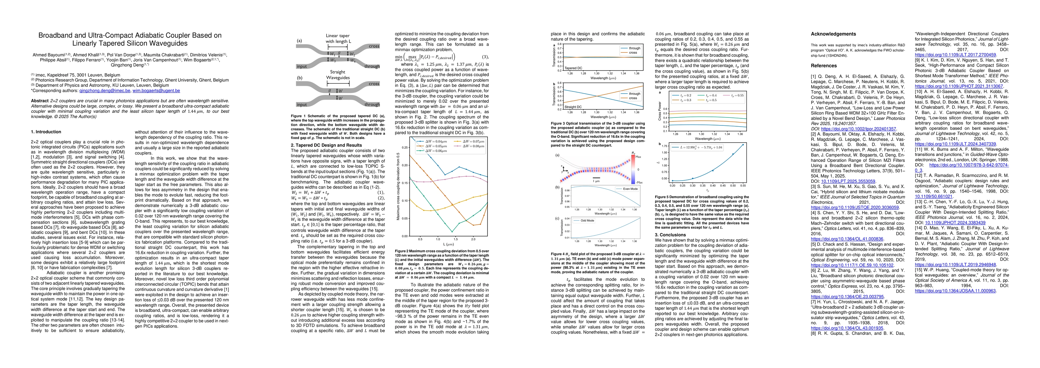
The research employs linearly tapered silicon waveguides to design a 2x2 adiabatic coupler, focusing on minimizing wavelength sensitivity and physical size.
Broadband and Ultra-Compact Adiabatic Coupler Based on Linearly Tapered Silicon Waveguides
Publication
Metrics
AI Quick Summary
This paper introduces a novel 2x2 broadband ultra-compact adiabatic coupler based on linearly tapered silicon waveguides, achieving minimal coupling variation and the shortest taper length of 1.44 µm, addressing the common issue of wavelength sensitivity in photonics applications.
Quick Answers
What is "Broadband and Ultra-Compact Adiabatic Coupler Based on Linearly Tapered Silicon Waveguides" about?
This paper introduces a novel 2x2 broadband ultra-compact adiabatic coupler based on linearly tapered silicon waveguides, achieving minimal coupling variation and the shortest taper length of 1.44 µm, addressing the common issue of wavelength sensitivity in photonics applications.
What methodology did the authors use?
The research employs linearly tapered silicon waveguides to design a 2x2 adiabatic coupler, focusing on minimizing wavelength sensitivity and physical size. More in Methodology →
What are the key results?
Presented a broadband ultra-compact adiabatic coupler with minimal coupling variation. — Achieved the least silicon taper length of 1.44 um, to the best knowledge of the authors. More in Key Results →
Why is this work significant?
This research is important as it offers a compact, broadband alternative to traditional wavelength-sensitive 2x2 couplers, which are often large, complex, or lossy, with potential applications in various photonics systems. More in Significance →
What are the main limitations?
The paper does not provide explicit information on potential limitations. — Real-world performance may depend on fabrication precision and material quality. More in Limitations →
Abstract
2x2 couplers are crucial in many photonics applications but are often wavelength-sensitive. Alternative designs could be large, complex, or lossy. We present a broadband ultra-compact adiabatic coupler with minimal coupling variation and the least silicon taper length of 1.44 um, to our best knowledge.
Key Findings, in focus
Seven facets of this paper, analysed and brought into focus by AI.
This research is important as it offers a compact, broadband alternative to traditional wavelength-sensitive 2x2 couplers, which are often large, complex, or lossy, with potential applications in various photonics systems.
- Presented a broadband ultra-compact adiabatic coupler with minimal coupling variation.
- Achieved the least silicon taper length of 1.44 um, to the best knowledge of the authors.
This research is important as it offers a compact, broadband alternative to traditional wavelength-sensitive 2x2 couplers, which are often large, complex, or lossy, with potential applications in various photonics systems.
The development of a novel linearly tapered silicon waveguide-based adiabatic coupler design with exceptional broadband characteristics and minimal footprint.
This work stands out due to its ultra-compact size and broadband performance, surpassing known alternatives in terms of silicon taper length and coupling variation.
- The paper does not provide explicit information on potential limitations.
- Real-world performance may depend on fabrication precision and material quality.
- Explore coupler performance under different environmental conditions.
- Investigate scalability to higher-dimensional photonic circuits.
Paper Details
Authors
PDF Preview
Related Papers
No references found for this paper.
Discussion 0