ArxivLens
ArXiv physics.app-ph

Broadband multilayer metasurface absorbers with MXene resonators and topology optimized substrates

Haozhe Wang, Maria Thaleia Passia, Steven A. Cummer, Yilin Zhao

2603.00657 2025 Nineteenth International Congress on Artificial Materials for Novel Wave Phenomena (Metamaterials) (2025) 263-265 DOI: 10.1109/Metamaterials65622.2025.11174171 Published Feb 28, 2026
View PDF

Publication

Published: Feb 28, 2026
Categories: physics.app-ph

Metrics

Source: ArXiv

Quick Answers

What methodology did the authors use?

Fabricated multilayer metamaterial absorbers using MXene resonators interleaved with dielectric layers, then applied density-based topology optimization in COMSOL to design dielectric substrate profiles, and used the BINACONN method to convert continuous designs into manufacturable binary resin/air patterns for SLA 3D printing. More in Methodology →

What are the key results?

Achieved an average absorbance of 91% over 10–19 GHz with the MXene-based multilayer MMA. — Topology-optimized dielectric substrates increased absorption compared to constant dielectric profiles. More in Key Results →

Why is this work significant?

The work demonstrates a versatile platform that combines high-loss MXene resonators with 3D-printed, topology-optimized substrates, enabling broadband, high-performance absorbers for radar, EMI shielding, and sensing applications. More in Significance →

What are the main limitations?

MXene conductivity is lower than copper, limiting maximum achievable loss. — 3D printing resolution constraints may restrict fine feature realization and exact dielectric profiles. More in Limitations →

Paper Preview

Abstract

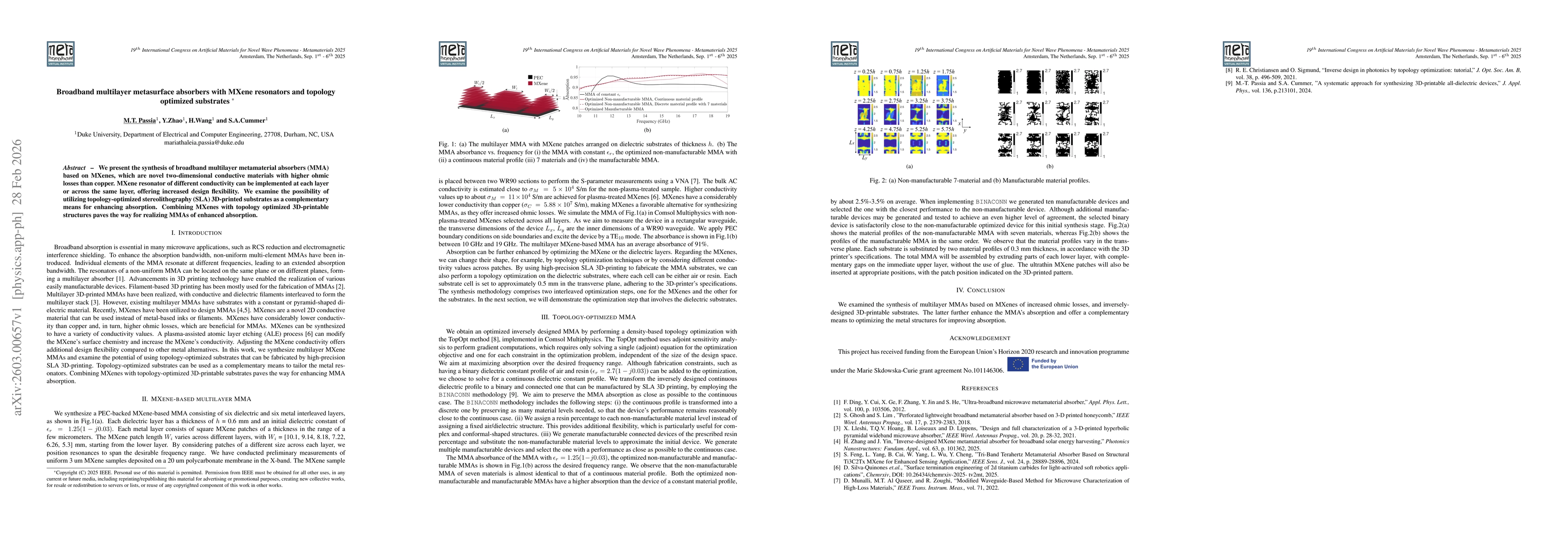
We present the synthesis of broadband multilayer metamaterial absorbers (MMA) based on MXenes, which are novel two-dimensional conductive materials with higher ohmic losses than copper. MXene resonator of different conductivity can be implemented at each layer or across the same layer, offering increased design flexibility. We examine the possibility of utilizing topology-optimized stereolithography (SLA) 3D-printed substrates as a complementary means for enhancing absorption. Combining MXenes with topology optimized 3D-printable structures paves the way for realizing MMAs of enhanced absorption.

Key Findings, in focus

Seven facets of this paper, analysed and brought into focus by AI.

AI-generated · verify against source Generated Mar 04, 2026
In focus · one-line synthesis

The work demonstrates a versatile platform that combines high-loss MXene resonators with 3D-printed, topology-optimized substrates, enabling broadband, high-performance absorbers for radar, EMI shielding, and sensing applications.

01
MethodologyHow they did it

Fabricated multilayer metamaterial absorbers using MXene resonators interleaved with dielectric layers, then applied density-based topology optimization in COMSOL to design dielectric substrate profiles, and used the BINACONN method to convert continuous designs into manufacturable binary resin/air patterns for SLA 3D printing.

02
ResultsWhat they found
  • Achieved an average absorbance of 91% over 10–19 GHz with the MXene-based multilayer MMA.
  • Topology-optimized dielectric substrates increased absorption compared to constant dielectric profiles.
  • Manufacturable binary substrates produced via BINACONN retained performance within 2.5–3.5% of the continuous optimized design.
03
SignificanceWhy it matters

The work demonstrates a versatile platform that combines high-loss MXene resonators with 3D-printed, topology-optimized substrates, enabling broadband, high-performance absorbers for radar, EMI shielding, and sensing applications.

04
Technical ContributionsWhat's new technically

Integration of MXene resonators with density-based topology optimization and the BINACONN manufacturability framework to produce high‑absorption, multilayer metamaterial absorbers on 3D‑printed substrates.

05
NoveltyWhat sets it apart

First demonstration of combining MXene-based multilayer absorbers with topology‑optimized, SLA‑printed dielectric substrates, providing unprecedented design flexibility and broadband absorption.

06
LimitationsWhat to be cautious about
  • MXene conductivity is lower than copper, limiting maximum achievable loss.
  • 3D printing resolution constraints may restrict fine feature realization and exact dielectric profiles.
07
Future WorkWhere it goes next
  • Fabricate and experimentally characterize the SLA-printed MMA to validate simulation results.
  • Investigate plasma-treated MXenes to increase conductivity and further enhance absorption.
  • Extend topology optimization to jointly optimize MXene geometry, conductivity distribution, and dielectric layout.

Paper Details

Paper ID: 2603.00657
Journal: 2025 Nineteenth International Congress on Artificial Materials for Novel Wave Phenomena (Metamaterials) (2025) 263-265
Comments: 4 pages, 2 figures, conference
Categories:
physics.app-ph

How to Cite This Paper

Reference manager: RIS EndNote


Discussion 0

This website uses cookies to ensure you get the best experience. Learn more