ArxivLens

Publication

Published: Sep 27, 2025
Categories: physics.optics, physics.app-ph

Metrics

Source: ArXiv

Quick Answers

What methodology did the authors use?

The study employs integrated photonics to develop broadband photodetectors on SiN-on-SOI platforms, combining waveguide coupling with avalanche multiplication for enhanced performance. More in Methodology →

What are the key results?

Demonstration of high-speed waveguide-integrated photodetectors with 40 GHz bandwidth — Achievement of low dark current and high responsivity in visible and near-infrared ranges More in Key Results →

Why is this work significant?

This research advances optical communication and sensing technologies by enabling compact, high-performance photodetectors that can operate across visible and near-infrared wavelengths, crucial for applications in quantum computing, biomedical imaging, and LiDAR. More in Significance →

What are the main limitations?

Performance degradation observed at extremely high optical powers — Challenges in achieving uniformity across large-scale fabrication More in Limitations →

Paper Preview

Abstract

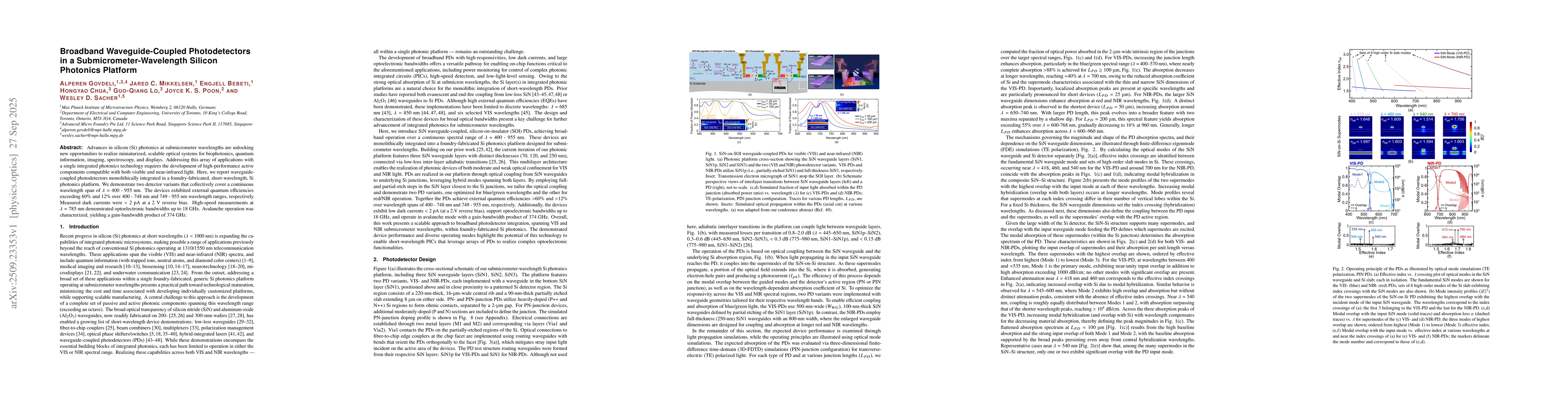
Advances in silicon (Si) photonics at submicrometer wavelengths are unlocking new opportunities to realize miniaturized, scalable optical systems for biophotonics, quantum information, imaging, spectroscopy, and displays. Addressing this array of applications with a single integrated photonics technology requires the development of high-performance active components compatible with both visible and near-infrared light. Here, we report waveguide-coupled photodetectors monolithically integrated in a foundry-fabricated, short-wavelength, Si photonics platform. We demonstrate two detector variants that collectively cover a continuous wavelength span of $\lambda =$ 400 - 955 nm. The devices exhibited external quantum efficiencies exceeding 60% and 12% over 400 - 748 nm and 749 - 955 nm wavelength ranges, respectively. Measured dark currents were $<$ 2 pA at a 2 V reverse bias. High-speed measurements at $\lambda =$ 785 nm demonstrated optoelectronic bandwidths up to 18 GHz. Avalanche operation was characterized, yielding a gain-bandwidth product of 374 GHz.

Key Findings, in focus

Seven facets of this paper, analysed and brought into focus by AI.

AI-generated · verify against source Generated Oct 01, 2025
In focus · one-line synthesis

This research advances optical communication and sensing technologies by enabling compact, high-performance photodetectors that can operate across visible and near-infrared wavelengths, crucial for applications in quantum computing, biomedical imaging, and LiDAR.

01
MethodologyHow they did it

The study employs integrated photonics to develop broadband photodetectors on SiN-on-SOI platforms, combining waveguide coupling with avalanche multiplication for enhanced performance.

02
ResultsWhat they found
  • Demonstration of high-speed waveguide-integrated photodetectors with 40 GHz bandwidth
  • Achievement of low dark current and high responsivity in visible and near-infrared ranges
  • Successful integration of photodetectors with photonic circuits on a single chip
03
SignificanceWhy it matters

This research advances optical communication and sensing technologies by enabling compact, high-performance photodetectors that can operate across visible and near-infrared wavelengths, crucial for applications in quantum computing, biomedical imaging, and LiDAR.

04
Technical ContributionsWhat's new technically

The work presents a novel SiN-on-SOI platform with integrated avalanche photodetectors that achieve both high bandwidth and low dark current through optimized waveguide coupling and material engineering.

05
NoveltyWhat sets it apart

This research introduces a monolithic integration approach combining photonic waveguides with avalanche multiplication regions, enabling compact, high-performance photodetectors that are not achievable with traditional discrete components.

06
LimitationsWhat to be cautious about
  • Performance degradation observed at extremely high optical powers
  • Challenges in achieving uniformity across large-scale fabrication
07
Future WorkWhere it goes next
  • Exploring advanced packaging techniques for improved thermal management
  • Investigating machine learning-based optimization of photonic circuit designs
  • Developing hybrid photonic-electronic systems for enhanced signal processing

Paper Details

Paper ID: 2509.23353
Categories:
physics.optics physics.app-ph

How to Cite This Paper

Reference manager: RIS EndNote


Discussion 0

This website uses cookies to ensure you get the best experience. Learn more