Bulk transport properties of Bismuth selenide thin films approaching the two-dimensional limit
Publication
Metrics
AI Quick Summary
This study investigates the transport properties of Bi2Se3 thin films as their thickness approaches the two-dimensional limit, revealing significant changes in bulk resistivity and Hall mobility below 6 quintuple layers due to an increased bulk band gap. The findings suggest potential for tunable properties in few-layer Bi2Se3, making it suitable for optoelectronics, nanoelectronics, and spintronics applications.
Paper Preview
Abstract
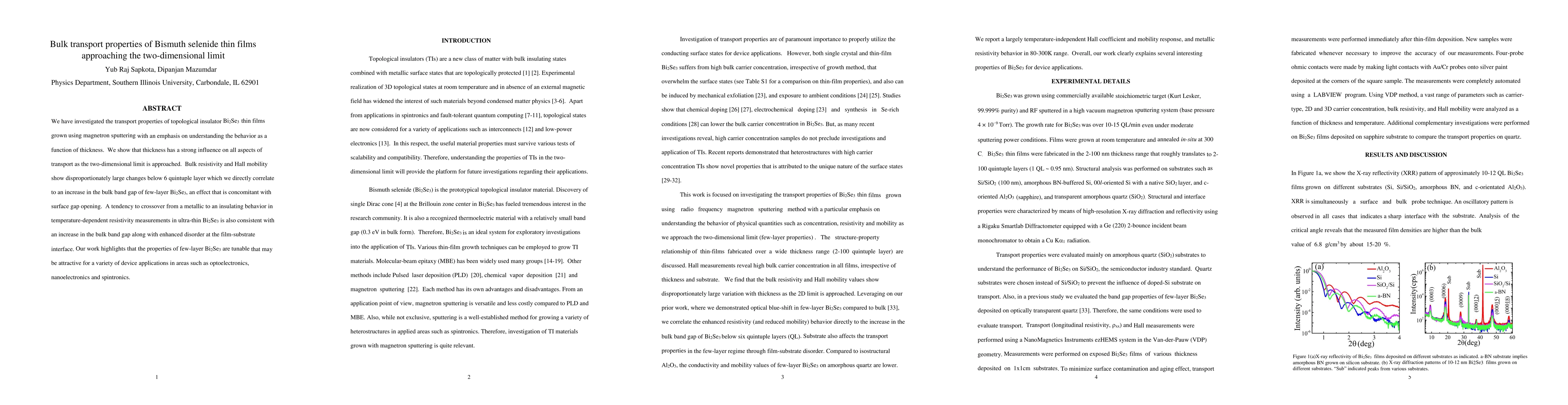
We have investigated the transport properties of topological insulator Bi2Se3 thin films grown using magnetron sputtering with an emphasis on understanding the behavior as a function of thickness. We show that thickness has a strong influence on all aspects of transport as the two-dimensional limit is approached. Bulk resistivity and Hall mobility show disproportionately large changes below 6 quintuple layer which we directly correlate to an increase in the bulk band gap of few-layer Bi2Se3, an effect that is concomitant with surface gap opening. A tendency to crossover from a metallic to an insulating behavior in temperature-dependent resistivity measurements in ultra-thin Bi2Se3 is also consistent with an increase in the bulk band gap along with enhanced disorder at the film-substrate interface. Our work highlights that the properties of few-layer Bi2Se3 are tunable that may be attractive for a variety of device applications in areas such as optoelectronics, nanoelectronics and spintronics.
AI Key Findings
Get AI-generated insights about this paper's methodology, results, significance, and more — seven facets brought into focus.
Impact
Paper Details
PDF Preview
Key Terms
Citation Network
Current paper (gray), citations (green), references (blue)
Display is limited for performance on very large graphs.
Discussion 0