ArxivLens

Publication

Published: Feb 24, 2025
Categories: cond-mat.mtrl-sci

Metrics

Source: ArXiv

AI Quick Summary

This research demonstrates that the carrier recombination rate in semiconductors with multi-level defects depends nonlinearly on the excess carrier density, contrary to the linear assumption in the traditional ABC model. Neglecting carrier emission from defects can lead to significant underestimations of recombination rates, suggesting a reformulation to the A(n)BC model.

Quick Answers

What is "Carrier Emission and Capture Competition mediated A(n)BC Recombination Model in Semiconductors with Multi-Level Defects" about?

This research demonstrates that the carrier recombination rate in semiconductors with multi-level defects depends nonlinearly on the excess carrier density, contrary to the linear assumption in the traditional ABC model. Neglecting carrier emission from defects can lead to significant underestimations of recombination rates, suggesting a reformulation to the A(n)BC model.

What methodology did the authors use?

The research employs first-principles calculations and a modified parallel-circuit recombination model to analyze multi-level defects in semiconductors, considering carrier emission effects. More in Methodology →

What are the key results?

Neglecting carrier emission can cause significant underestimation of the recombination rate by over 8 orders of magnitude for high excess carrier densities. — The recombination coefficient A is a function of carrier density (A(n)), not constant, for multi-level defects. More in Key Results →

Why is this work significant?

This study highlights the importance of considering carrier emission in multi-level defect recombination, which can lead to more accurate predictions in the design of optoelectronic devices such as LEDs and solar cells. More in Significance →

What are the main limitations?

The study focuses on theoretical calculations and does not include experimental validation. — The analysis is limited to specific defects (V_Ga-O_N in GaN and Pb_I in CsPbI_3) and may not generalize to all multi-level defects in semiconductors. More in Limitations →

Paper Preview

Abstract

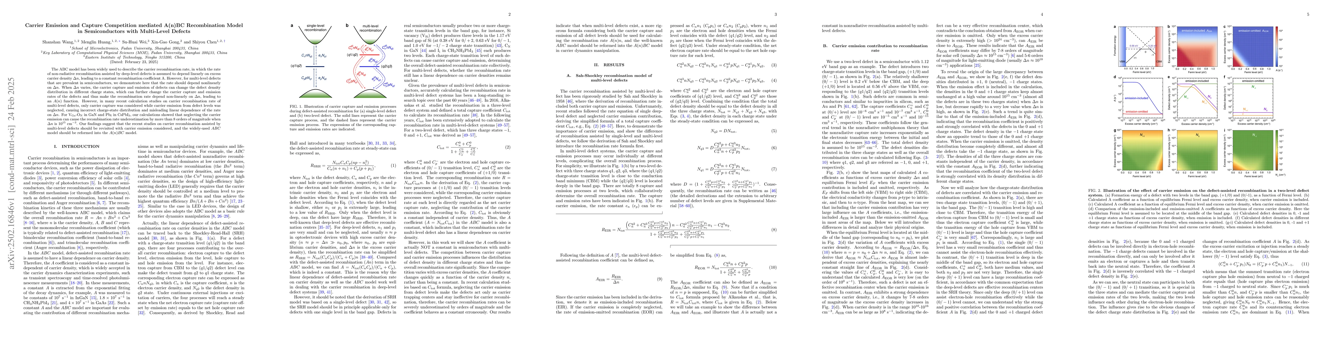
The ABC model has been widely used to describe the carrier recombination rate, in which the rate of non-radiative recombination assisted by deep-level defects is assumed to depend linearly on excess carrier density $\Delta n$, leading to a constant recombination coefficient A. However, for multi-level defects that are prevalent in semiconductors, we demonstrate here that the rate should depend nonlinearly on $\Delta n$. When $\Delta n$ varies, the carrier capture and emission of defects can change the defect density distribution in different charge states, which can further change the carrier capture and emission rates of the defects and thus make the recombination rate depend non-linearly on $\Delta n$, leading to an $A(n)$ function. However, in many recent calculation studies on carrier recombination rate of multi-level defects, only carrier capture was considered while carrier emission from defect levels was neglected, causing incorrect charge-state distribution and misleading linear dependence of the rate on $\Delta n$. For $\text{V}_{\text{Ga}}$-$\text{O}_{\text{N}}$ in GaN and $\text{Pb}_\text{I}$ in CsPbI$_3$, our calculations showed that neglecting the carrier emission can cause the recombination rate underestimation by more than 8 orders of magnitude when $\Delta n$ is $10^{15}$ cm$^{-3}$. Our findings suggest that the recent studies on carrier recombination assisted by multi-level defects should be revisited with carrier emission considered, and the widely-used $ABC$ model should be reformed into the $A(n)BC$ model.
Key Findings, in focus

Seven facets of this paper, analysed and brought into focus by AI.

AI-generated · verify against source Generated Jun 11, 2025
In focus · one-line synthesis

This study highlights the importance of considering carrier emission in multi-level defect recombination, which can lead to more accurate predictions in the design of optoelectronic devices such as LEDs and solar cells.

01
MethodologyHow they did it

The research employs first-principles calculations and a modified parallel-circuit recombination model to analyze multi-level defects in semiconductors, considering carrier emission effects.

02
ResultsWhat they found
  • Neglecting carrier emission can cause significant underestimation of the recombination rate by over 8 orders of magnitude for high excess carrier densities.
  • The recombination coefficient A is a function of carrier density (A(n)), not constant, for multi-level defects.
  • The traditional ABC recombination model should be reformed into the A(n)BC model to accurately describe recombination assisted by multi-level defects.
03
SignificanceWhy it matters

This study highlights the importance of considering carrier emission in multi-level defect recombination, which can lead to more accurate predictions in the design of optoelectronic devices such as LEDs and solar cells.

04
Technical ContributionsWhat's new technically

The paper proposes a modified parallel-circuit recombination model that includes carrier emission effects, providing a more accurate description of recombination in semiconductors with multi-level defects.

05
NoveltyWhat sets it apart

The research distinguishes itself by emphasizing the nonlinear dependence of recombination rate on excess carrier density (A(n)) due to carrier capture and emission competition in multi-level defects, contrasting with the traditional constant recombination coefficient (A) assumption.

06
LimitationsWhat to be cautious about
  • The study focuses on theoretical calculations and does not include experimental validation.
  • The analysis is limited to specific defects (V_Ga-O_N in GaN and Pb_I in CsPbI_3) and may not generalize to all multi-level defects in semiconductors.
07
Future WorkWhere it goes next
  • Revisit recent calculation studies on carrier recombination assisted by multi-level defects, incorporating carrier emission effects.
  • Extend the findings to a broader range of semiconductor materials and multi-level defects.

Impact

70
References

Paper Details

Paper ID: 2502.16846
Categories:
cond-mat.mtrl-sci

How to Cite This Paper

Reference manager: RIS EndNote


Discussion 0

This website uses cookies to ensure you get the best experience. Learn more