Authors
Summary
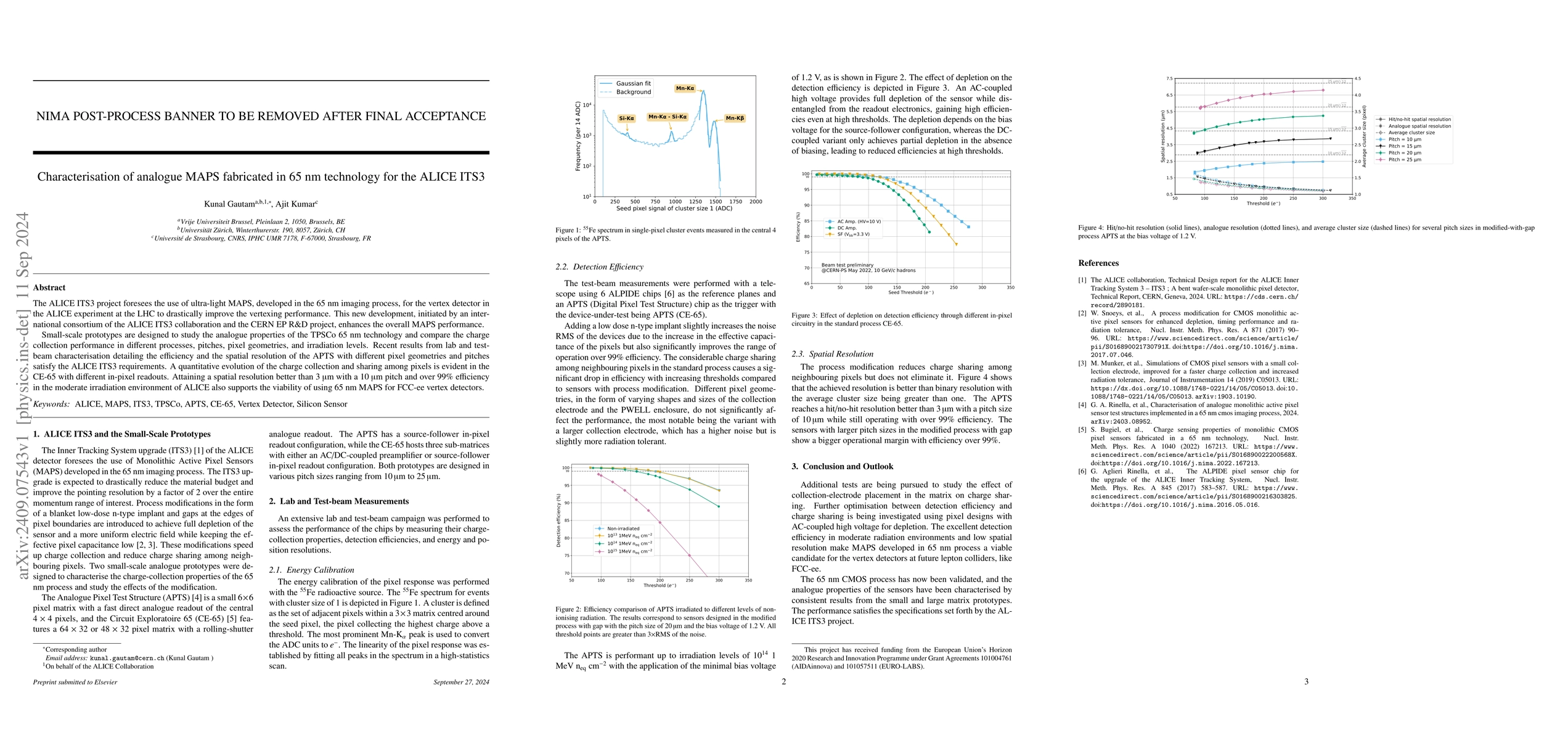
The ALICE ITS3 project foresees the use of ultra-light MAPS, developed in the 65 nm imaging process, for the vertex detector in the ALICE experiment at the LHC to drastically improve the vertexing performance. This new development, initiated by an international consortium of the ALICE ITS3 collaboration and the CERN EP R&D project, enhances the overall MAPS performance. Small-scale prototypes are designed to study the analogue properties of the TPSCo 65 nm technology and compare the charge collection performance in different processes, pitches, pixel geometries, and irradiation levels. Recent results from lab and test-beam characterisation detailing the efficiency and the spatial resolution of the APTS with different pixel geometries and pitches satisfy the ALICE ITS3 requirements. A quantitative evolution of the charge collection and sharing among pixels is evident in the CE-65 with different in-pixel readouts. Attaining a spatial resolution better than 3 $\mu$m with a 10 $\mu$m pitch and over 99% efficiency in the moderate irradiation environment of ALICE also supports the viability of using 65 nm MAPS for FCC-ee vertex detectors.
AI Key Findings
Generated Sep 05, 2025
Methodology
The research employed a combination of lab and test-beam measurements to assess the performance of the 65 nm MAPS fabricated in the ALICE ITS3 project.
Key Results
- Main finding: The APTS with different pixel geometries and pitches satisfies the ALICE ITS3 requirements, achieving a spatial resolution better than 3 μm with over 99% efficiency.
- Main finding: The CE-65 features a rolling-shutter configuration, which improves the detection efficiency in moderate irradiation environments.
- Main finding: The process modification reduces charge sharing among neighboring pixels but does not eliminate it, resulting in a higher operational margin.
Significance
This research is important as it validates the 65 nm CMOS process for MAPS development and demonstrates their potential for use in vertex detectors at future lepton colliders.
Technical Contribution
The research presents a detailed characterization of the analogue MAPS fabricated in 65 nm technology, highlighting their potential for use in vertex detectors at future lepton colliders.
Novelty
This work contributes to the development of ultra-light MAPS using the 65 nm CMOS process, which is a novel approach to improving vertexing performance in particle detectors.
Limitations
- The small-scale prototypes may not accurately represent the full-scale detector performance.
- Further optimization between detection efficiency and charge sharing is needed.
Future Work
- Investigating the effect of collection-electrode placement in the matrix on charge sharing.
- Developing pixel designs with AC-coupled high-voltage for depletion to further improve detection efficiency.
Paper Details
PDF Preview
Citation Network
Current paper (gray), citations (green), references (blue)
Display is limited for performance on very large graphs.
Similar Papers
Found 4 papersCharacterisation of analogue MAPS produced in the 65 nm TPSCo process
Armin Ilg, Anna Macchiolo, Eduardo Ploerer et al.
Simulations and Performance Studies of a MAPS in 65 nm CMOS Imaging Technology
Adriana Simancas, Justus Braach, Eric Buschmann et al.
Further Characterisation of Digital Pixel Test Structures Implemented in a 65 nm CMOS Process
Edoardo Charbon, Peter Svihra, Vittorio Di Trapani et al.
BabyMOSS stitched sensors: results of characterisation tests for ALICE ITS3 upgrade
Alessandro Sturniolo
| Title | Authors | Year | Actions |
|---|
Comments (0)