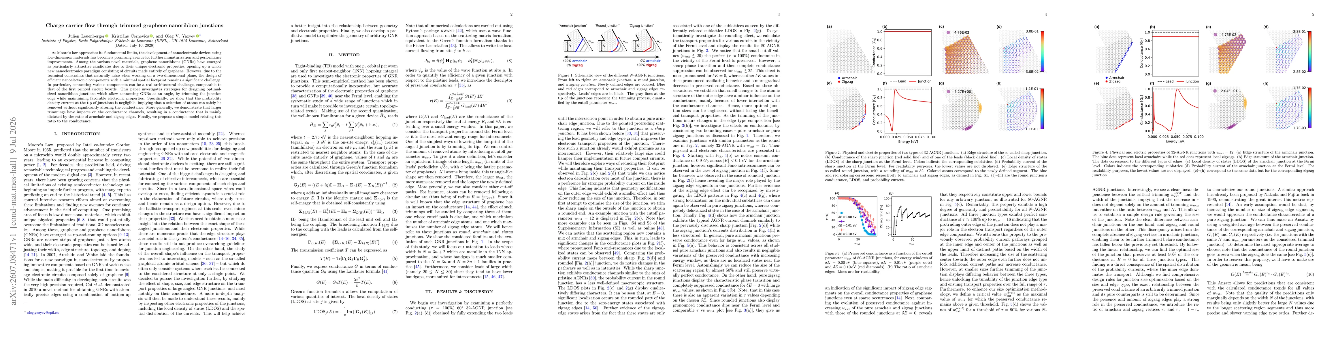
The study employs a tight-binding model with one pz orbital per atom and first-nearest-neighbor hopping to evaluate electronic transport in graphene nanoribbon (GNR) junctions. Conductance is computed via Green’s function formalism, using self-energies from leads and the Landauer approach, implemented in Kwant for numerical calculations. A trimming parameter wext is introduced to remove atoms along specific cutoff paths (equilateral-triangle, circular arc, armchair-maximizing, zigzag-maximizing) to study effects on conductance, LDOS, and current distribution. A simple model relating the conductance to the armchair/zigzag edge ratio is proposed to predict transport changes due to trimming.
Charge carrier flow through trimmed graphene nanoribbon junctions
Publication
Metrics
Quick Answers
What methodology did the authors use?
The study employs a tight-binding model with one pz orbital per atom and first-nearest-neighbor hopping to evaluate electronic transport in graphene nanoribbon (GNR) junctions. Conductance is computed via Green’s function formalism, using self-energies from leads and the Landauer approach, implemented in Kwant for numerical calculations. A trimming parameter wext is introduced to remove atoms along specific cutoff paths (equilateral-triangle, circular... More in Methodology →
What are the key results?
Trimming the junction tip yields negligible current density at the tip, indicating safe removal of atoms without major conductance degradation for small trims. — Larger trim sizes progressively alter conductance channels and drive conductance to be governed mainly by the relative ratio of armchair and zigzag edge atoms. More in Key Results →
Why is this work significant?
Provides actionable guidelines for engineering graphene nanoribbon junctions with angled connections by edge trimming, enabling preserved or tunable conductance while allowing geometric flexibility in nanoelectronic circuit layouts. More in Significance →
What are the main limitations?
Study relies on a 1NN tight-binding model which may omit longer-range interactions and edge-passivation effects that can influence real-world conductance. — Assumes ideal leads and pristine edges; disorder, defects, and substrate interactions are not explicitly addressed. More in Limitations →
Abstract
As Moore's law approaches its fundamental limits, the development of nanoelectronic devices using low-dimension materials has become a promising avenue for further miniaturization and performance improvements. Among the various novel materials, graphene nanoribbons (GNRs) have emerged as particularly attractive candidates due to their unique electronic properties, opening up a whole new nanoelectronics paradigm consisting of circuits made entirely of graphene. However, due to the technical constraints that naturally arise when working on a two-dimensional plane, the design of efficient nanoelectronic components with a minimal spatial footprint remains a significant challenge. In particular, connecting various components can be a real architectural challenge, comparable to that of the first printed circuit boards. This paper investigates strategies for designing optimal-sized nanoribbon junctions which allow connecting GNRs at an angle, by trimming the junction edge while maintaining favorable electronic properties. Specifically, we show that the probability density current at the tip of junctions is negligible, implying that a selection of atoms can safely be removed without significantly altering the conductance. More generally, we demonstrate that larger trimmings have impacts on the conductance channels, resulting in a conductance that is mainly dictated by the ratio of armchair and zigzag edges. Finally, we propose a simple model relating this ratio to the conductance.
Key Findings, in focus
Seven facets of this paper, analysed and brought into focus by AI.
Provides actionable guidelines for engineering graphene nanoribbon junctions with angled connections by edge trimming, enabling preserved or tunable conductance while allowing geometric flexibility in nanoelectronic circuit layouts.
- Trimming the junction tip yields negligible current density at the tip, indicating safe removal of atoms without major conductance degradation for small trims.
- Larger trim sizes progressively alter conductance channels and drive conductance to be governed mainly by the relative ratio of armchair and zigzag edge atoms.
- A simple predictive model links the conductance to the armchair/zigzag edge ratio, offering a guideline for designing angled GNR junctions with preserved transport properties.
Provides actionable guidelines for engineering graphene nanoribbon junctions with angled connections by edge trimming, enabling preserved or tunable conductance while allowing geometric flexibility in nanoelectronic circuit layouts.
Proposes a systematic trimming framework (wext-based) for GNR junctions and demonstrates its impact on conductance via Green’s-function transport, plus a simple edge-ratio model that relates trimming-induced changes in conductance to the armchair/zigzag edge composition.
Introduces the concept of edge trimming as a design knob for angled GNR junctions and identifies a quantitative link between edge topology (armchair vs zigzag) and conductance, enabling geometry-driven optimization absent in prior analyses.
- Study relies on a 1NN tight-binding model which may omit longer-range interactions and edge-passivation effects that can influence real-world conductance.
- Assumes ideal leads and pristine edges; disorder, defects, and substrate interactions are not explicitly addressed.
- Extend the model to include next-nearest-neighbor interactions and edge passivation to assess robustness of trimming strategies.
- Explore trim effects under disorder, temperature variations, and environmental perturbations to evaluate practical reliability.
- Validate the predictive armchair/zigzag ratio model against larger datasets and experimental measurements to calibrate its applicability.
Discussion 0