01
MethodologyHow they did it
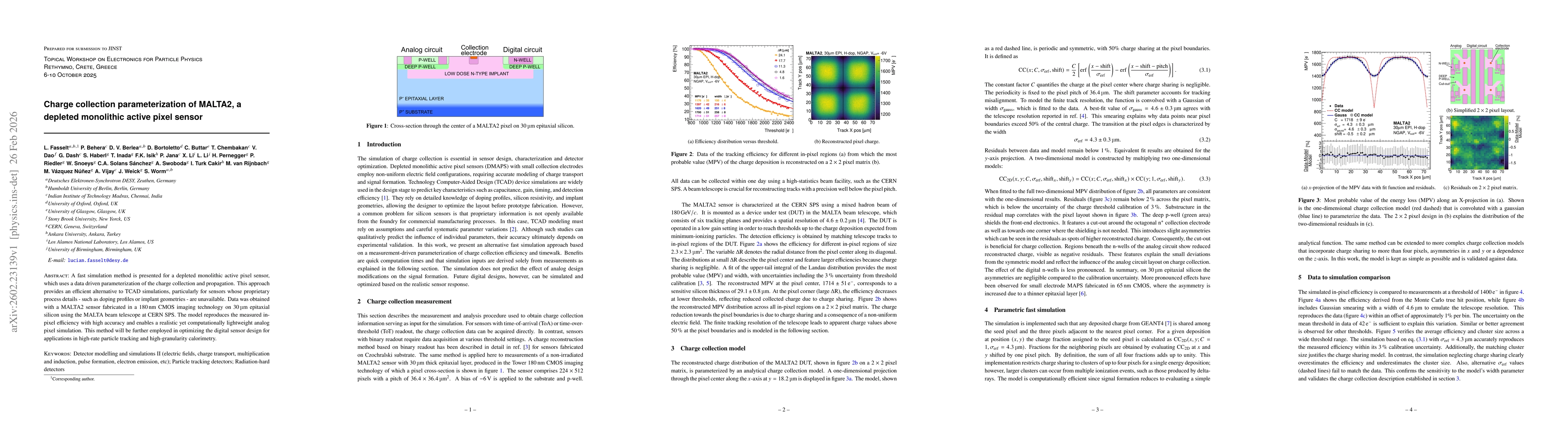
Beam test data from a MALTA2 sensor in a 180 nm CMOS process were used to parameterize charge collection with an analytical erf‑based model, convolved with a Gaussian to account for telescope resolution; the resulting function was implemented in a fast simulation that distributes deposited charge among up to four pixels.
Discussion 0