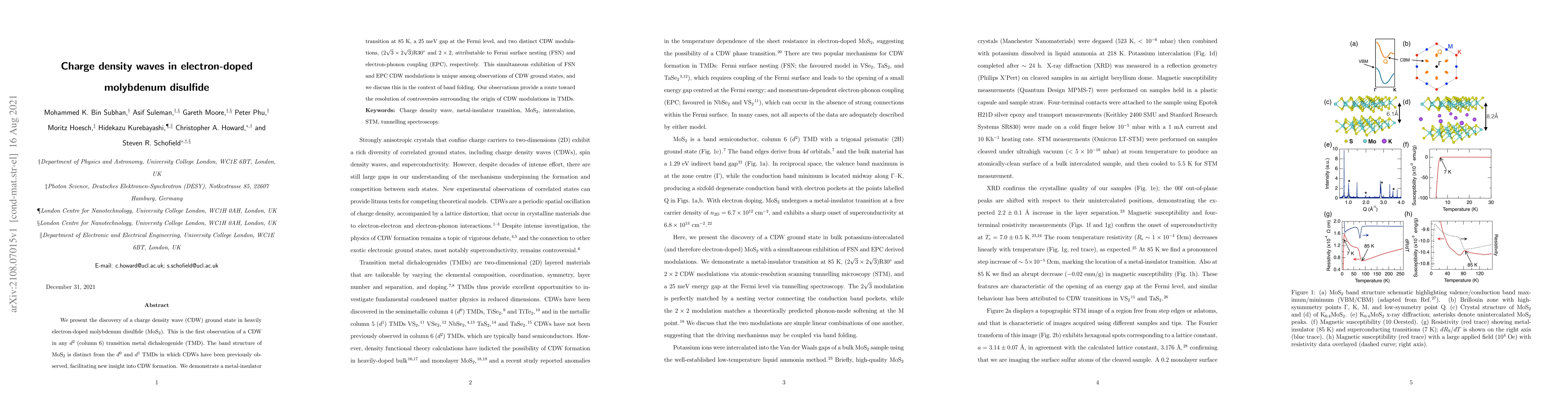
Charge density waves in electron-doped molybdenum disulfide
Publication
Metrics
AI Quick Summary
This paper reports the first observation of a charge density wave (CDW) in electron-doped molybdenum disulfide (MoS$_2$), revealing a metal-insulator transition at 85 K and a 25 meV gap. The study identifies two distinct CDW modulations, providing new insights into CDW formation in $d^2$ transition metal dichalcogenides.
Paper Preview
Abstract
We present the discovery of a charge density wave (CDW) ground state in heavily electron-doped molybdenum disulfide (MoS$_2$). This is the first observation of a CDW in any $d^2$ (column 6) transition metal dichalcogenide (TMD). The band structure of MoS$_2$ is distinct from the $d^0$ and $d^1$ TMDs in which CDWs have been previously observed, facilitating new insight into CDW formation. We demonstrate a metal-insulator transition at 85 K, a 25 meV gap at the Fermi level, and two distinct CDW modulations, $(2\sqrt{3}\times2\sqrt{3})$R$30^\circ$ and $2\times2$, attributable to Fermi surface nesting (FSN) and electron-phonon coupling (EPC), respectively. This simultaneous exhibition of FSN and EPC CDW modulations is unique among observations of CDW ground states, and we discuss this in the context of band folding. Our observations provide a route toward the resolution of controversies surrounding the origin of CDW modulations in TMDs.
AI Key Findings
Get AI-generated insights about this paper's methodology, results, significance, and more — seven facets brought into focus.
Impact
Paper Details
Authors
PDF Preview
Key Terms
Citation Network
Current paper (gray), citations (green), references (blue)
Display is limited for performance on very large graphs.
Discussion 0