Charge-noise-free Lateral Quantum Dot Devices with Undoped Si/SiGe Wafer
Publication
Metrics
AI Quick Summary
This study develops charge-noise-free quantum dots using an undoped Si/SiGe wafer, achieving clear Coulomb diamonds and double dot charge stability. Fourier transform analysis reveals that the noise power spectrum is inversely proportional to frequency, differing from doped wafers where noise is linked to 2DEG dopants.
Paper Preview
Abstract
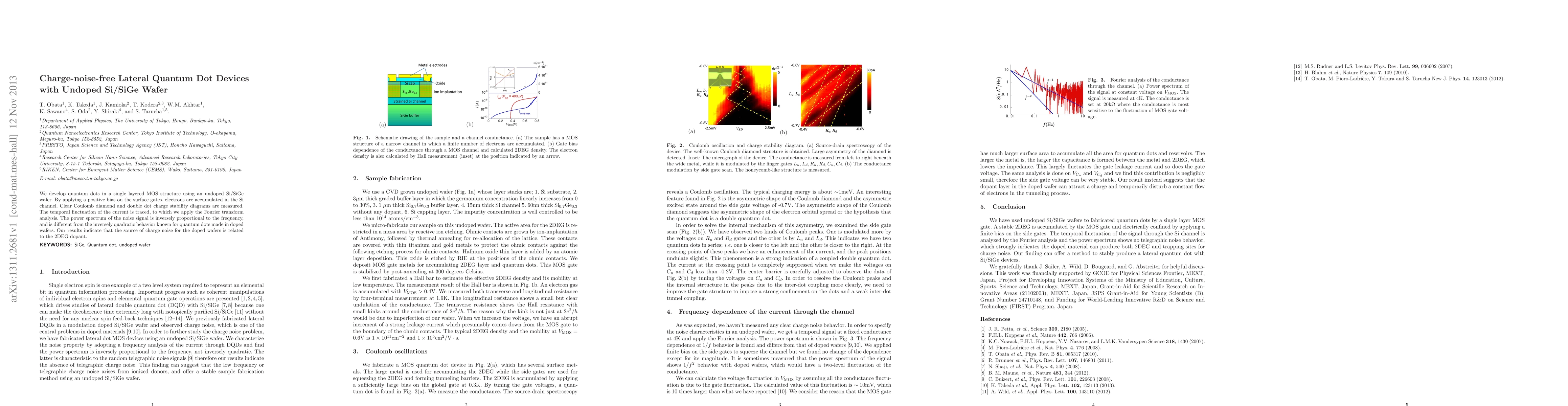
We develop quantum dots in a single layered MOS structure using an undoped Si/SiGe wafer. By applying a positive bias on the surface gates, electrons are accumulated in the Si channel. Clear Coulomb diamond and double dot charge stability diagrams are measured. The temporal fluctuation of the current is traced, to which we apply the Fourier transform analysis. The power spectrum of the noise signal is inversely proportional to the frequency, and is different from the inversely quadratic behavior known for quantum dots made in doped wafers. Our results indicate that the source of charge noise for the doped wafers is related to the 2DEG dopant.
AI Key Findings
Get AI-generated insights about this paper's methodology, results, significance, and more — seven facets brought into focus.
Impact
Paper Details
PDF Preview
Key Terms
Citation Network
Current paper (gray), citations (green), references (blue)
Display is limited for performance on very large graphs.
Discussion 0