01
MethodologyHow they did it
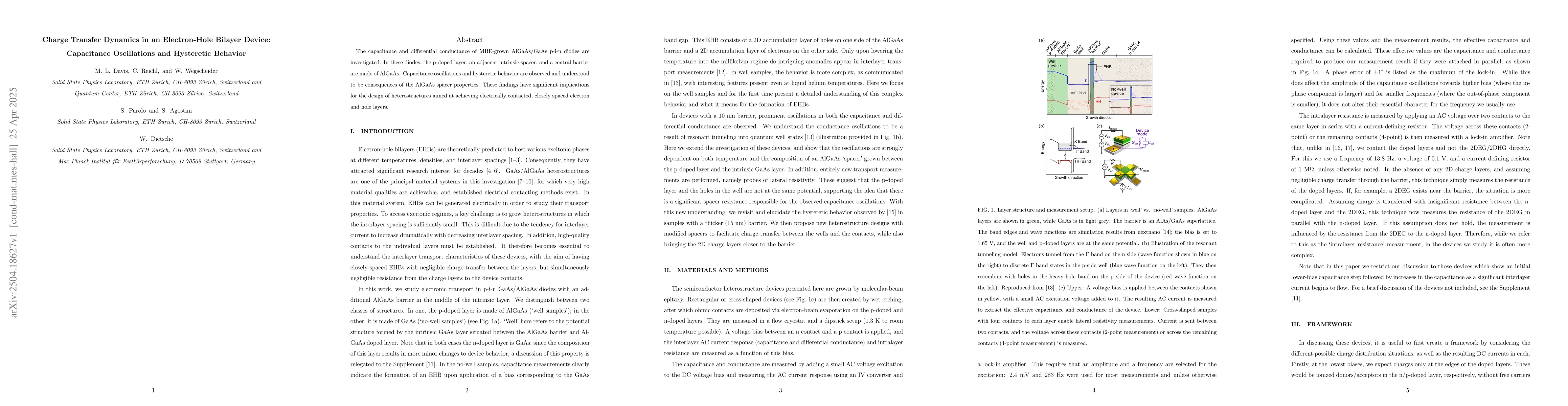
The research investigates capacitance and differential conductance of MBE-grown AlGaAs/GaAs p-i-n diodes, focusing on AlGaAs spacer properties and their impact on capacitance oscillations and hysteretic behavior in electron-hole bilayer devices.
Discussion 0