Cleaning Interfaces in Layered Materials Heterostructures
Publication
Metrics
AI Quick Summary
This paper presents a method to remove contaminants and blisters from interfaces in layered material heterostructures, achieving clean graphene interfaces encapsulated in hexagonal boron nitride with high electron mobilities. The technique is shown to work for graphene and MoS$_2$ heterostructures, indicating its general applicability and potential for fabricating high-performance (opto)-electronic devices.
Paper Preview
Abstract
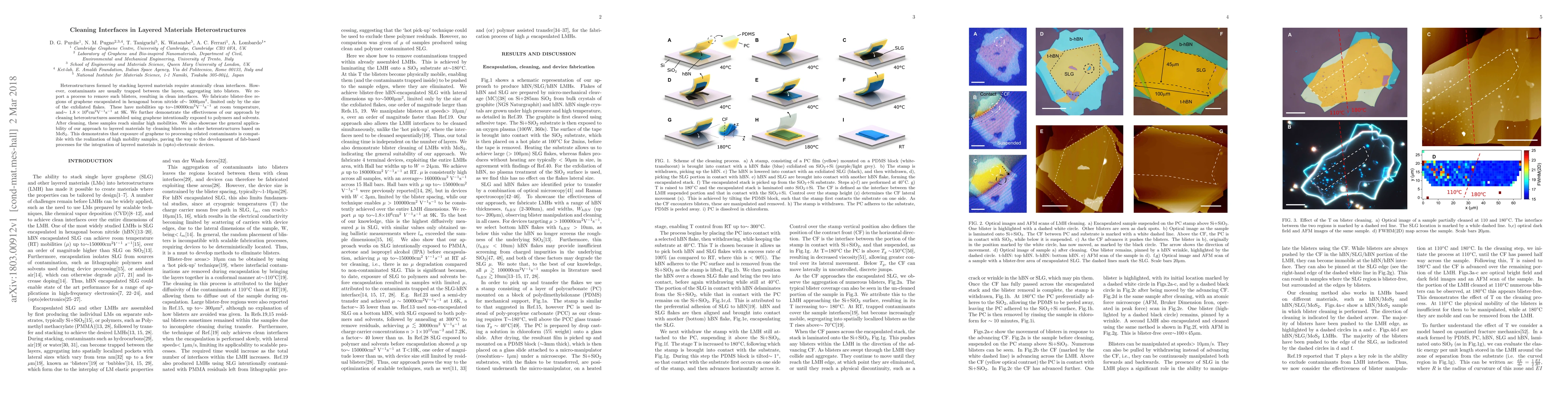
Heterostructures formed by stacking layered materials require atomically clean interfaces. However, contaminants are usually trapped between the layers, aggregating into blisters. We report a process to remove such blisters, resulting in clean interfaces. We fabricate blister-free regions of graphene encapsulated in hexagonal boron nitride of$\sim$5000$\mu $m$^{2}$, limited only by the size of the exfoliated flakes. These have mobilities up to$\sim$180000cm$^2$V$^{-1}$s$^{-1}$ at room temperature, and$\sim$1.8$\times$10$^6$cm$^2$V$^{-1}$s$^{-1}$ at 9K. We further demonstrate the effectiveness of our approach by cleaning heterostructures assembled using graphene intentionally exposed to polymers and solvents. After cleaning, these samples reach similar high mobilities. We also showcase the general applicability of our approach to layered materials by cleaning blisters in other heterostructures based on MoS$_{2}$. This demonstrates that exposure of graphene to processing-related contaminants is compatible with the realization of high mobility samples, paving the way to the development of fab-based processes for the integration of layered materials in (opto)-electronic devices.
AI Key Findings
Get AI-generated insights about this paper's methodology, results, significance, and more — seven facets brought into focus.
Impact
Paper Details
PDF Preview
Key Terms
Citation Network
Current paper (gray), citations (green), references (blue)
Display is limited for performance on very large graphs.
Discussion 0