01
MethodologyHow they did it
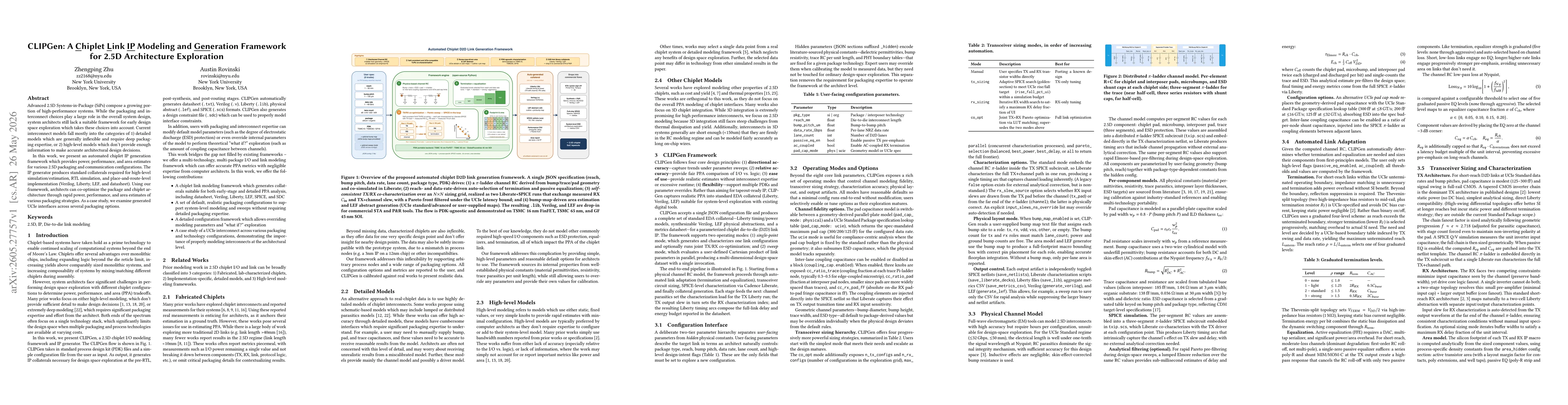
CLIPGen automates chiplet IP generation for 2.5D architectures by ingesting process design kit files and a simple user configuration to produce IP collaterals (Verilog, Liberty, LEF, datasheet, SPICE, SDC). It combines a distributed pi-ladder channel RC model with self-consistent TX/RX co-characterization across an N×N sizing grid, enabling quick power, performance, and area estimates across packaging options. The framework supports multi-PDKs and allows parameter overrides for what-if exploration, delivering drop-in collateral for industry STA and P&R tools to enable architectural design space exploration.
Discussion 0