Publication
Metrics
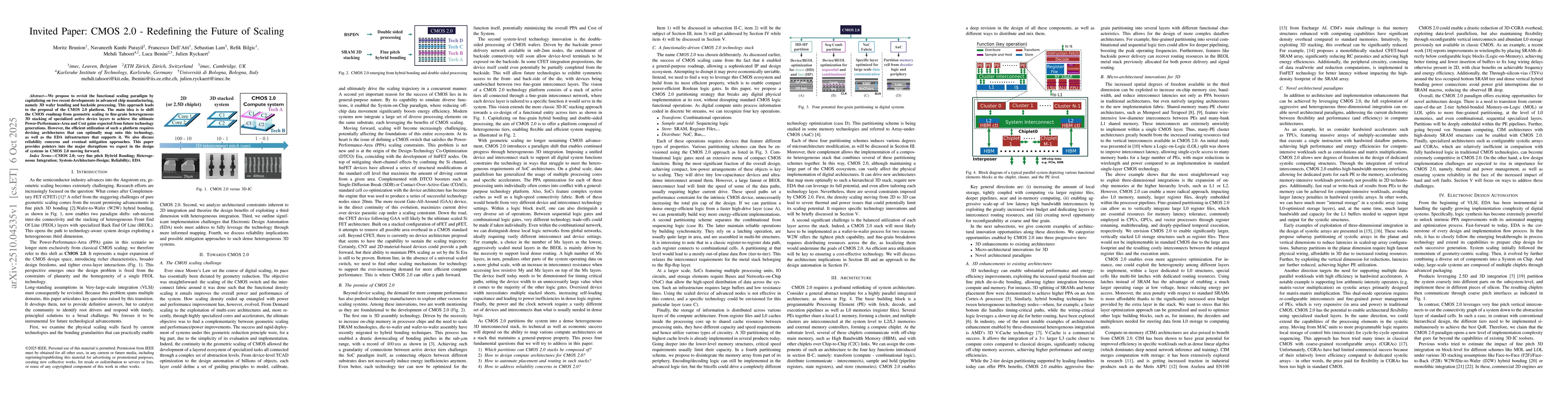
Paper Preview
Abstract
We propose to revisit the functional scaling paradigm by capitalizing on two recent developments in advanced chip manufacturing, namely 3D wafer bonding and backside processing. This approach leads to the proposal of the CMOS 2.0 platform. The main idea is to shift the CMOS roadmap from geometric scaling to fine-grain heterogeneous 3D stacking of specialized active device layers to achieve the ultimate Power-Performance-Area and Cost gains expected from future technology generations. However, the efficient utilization of such a platform requires devising architectures that can optimally map onto this technology, as well as the EDA infrastructure that supports it. We also discuss reliability concerns and eventual mitigation approaches. This paper provides pointers into the major disruptions we expect in the design of systems in CMOS 2.0 moving forward.
AI Key Findings — Processing
Key findings are being generated. Please check back in a few minutes.
Discussion 0