Quick Summary:

This paper presents a CMOS-compatible method for achieving controlled hyperdoping of silicon nanowires using non-equilibrium processing, which enables dopant concentrations far exceeding equilibrium levels. The technique involves nanoscale implantation and rapid annealing, resulting in Se-hyperdoped Si/SiO2 core/shell nanowires with a sub-band gap photoresponse, demonstrating potential for improving solar cell efficiency.

Summary

Hyperdoping consists of the intentional introduction of deep-level dopants into a semiconductor in excess of equilibrium concentrations. This causes a broadening of dopant energy levels into an intermediate band between the valence and conduction bands.[1,2] Recently, bulk Si hyperdoped with chalcogens or transition metals has been demonstrated to be an appropriate intermediate-band material for Si-based short-wavelength infrared photodetectors.[3-5] Intermediate-band nanowires could potentially be used instead of bulk materials to overcome the Shockley-Queisser limit and to improve efficiency in solar cells,[6-9] but fundamental scientific questions in hyperdoping Si nanowires require experimental verification. The development of a method for obtaining controlled hyperdoping levels at the nanoscale concomitant with the electrical activation of dopants is, therefore, vital to understanding these issues. Here, we show a CMOS-compatible technique based on non-equilibrium processing for the controlled doping of Si at the nanoscale with dopant concentrations several orders of magnitude greater than the equilibrium solid solubility. Through the nanoscale spatially controlled implantation of dopants, and a bottom-up template-assisted solid phase recrystallization of the nanowires with the use of millisecond-flash lamp annealing, we form Se-hyperdoped Si/SiO2 core/shell nanowires that have a room-temperature sub-band gap optoelectronic photoresponse when configured as a photoconductor device.
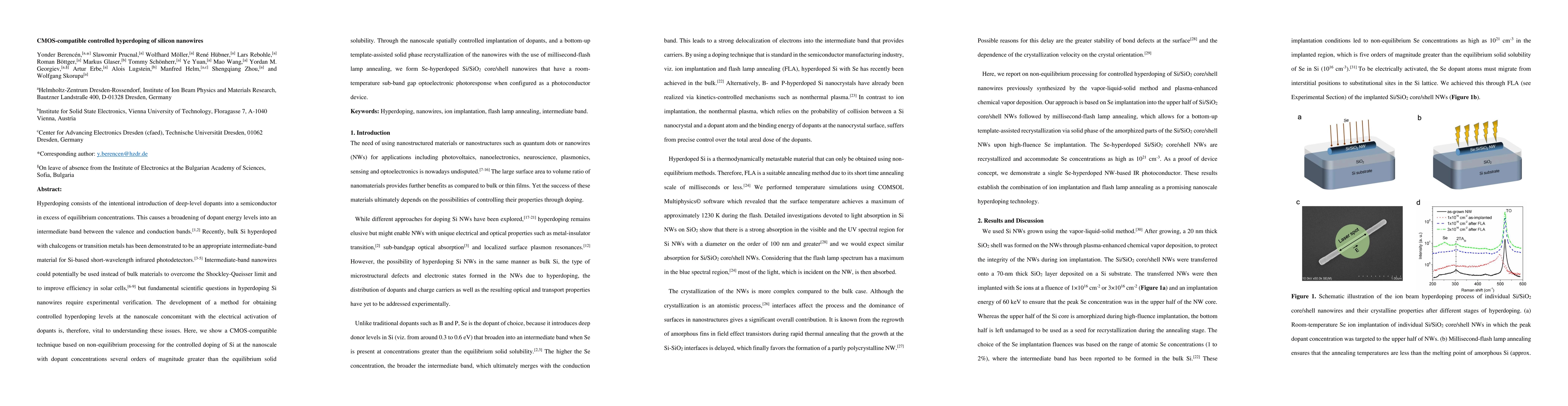
AI Key Findings

Get AI-generated insights about this paper's methodology, results, and significance.

Paper Details

PDF Preview

Download PDF

Key Terms

nanowires (0.284)
si (0.266)
nanoscale (0.231)
controlled (0.190)
band (0.189)
concentrations (0.188)
intermediate (0.176)
solid (0.167)
equilibrium (0.164)
levels (0.145)
bulk (0.144)
band gap (0.116)
annealing (0.114)
template (0.113)
valence (0.113)
conduction (0.113)
room temperature (0.112)
verification (0.111)
vital (0.110)
doping (0.110)

Citation Network

Current paper (gray), citations (green), references (blue)

Current Paper
Citations
References
Click to view
Title Authors Year Actions
Enhanced Activation in Phosphorous-Doped Silicon via Dual-Beam Laser Annealing
Rasheed Ayinde Taiwo, Yeongil Son, Joonghan Shin, Y. A. Salawu
2024
View Paper
Tunable magneto-transport properties in ultra-high Bi-doped Si prepared by liquid phase epitaxy
Mao Wang, Hang Liu, M. S. Shaikh, R. Heller, U. Kentsch, Ling Li, Shengqiang Zhou
2024
View Paper
Electrical transport properties in Ge hyperdoped with Te
D. Caudevilla, S. Algaidy, F. Pérez‐Zenteno, S. Duarte‐Cano, R. García‐Hernansanz, J. Olea, E. San Andrés, Á. del Prado, R. Barrio, I. Torres, E. García‐Hemme, D. Pastor
2022
View Paper
Hyperdoped silicon: Processing, properties, and devices
Zhouyu Tong, Mingxuan Bu, Yiqiang Zhang, Deren Yang, X. Pi
2022
View Paper
Room‐Temperature Infrared Photoresponse from Ion Beam–Hyperdoped Silicon
Mao Wang, Y. Berencén
2020
View Paper
Nanowire Electronics: From Nanoscale to Macroscale.
Chuancheng Jia, Zhaoyang Lin, Yu Huang, X. Duan
2019
View Paper
Joining of two different ceramic nanomaterials for bottom-up fabrication of heterojunction devices
M. Rajbhar, Pritam Das, B. Satpati, W. Möller, S. Facsko, R. Böttger, N. Ramgir, S. Chatterjee
2019
View Paper
Incorporation of Europium into GaN Nanowires by Ion Implantation
D. Faye, X. Biquard, E. Nogales, M. Felizardo, M. Peres, A. Redondo-Cubero, T. Auzelle, B. Daudin, L. Tizei, M. Kociak, P. Ruterana, W. Möller, B. Méndez, E. Alves, K. Lorenz
2019
View Paper
Formation of n- and p-type regions in individual Si/SiO2 core/shell nanowires by ion beam doping
Y. Berencén, S. Prucnal, Wolfhard Möller, R. Hübner, L. Rebohle, T. Schönherr, M. B. Khan, Mao Wang, M. Glaser, Y. Georgiev, Artur Erbe, A. Lugstein, M. Helm, Shijie Zhou
2018
View Paper
Helmholtz-Zentrum Dresden-Rossendorf (HZDR) Extended Infrared Photoresponse in Te-Hyperdoped Si at Room Temperature
Mao Wang, Y. Berenc'en, E. Garc'ia-Hemme, S. Prucnal, R. Hübner, Ye Yuan, Chi Xu, L. Rebohle, R. Böttger, R. Heller, H. Schneider, W. Skorupa, M. Helm, Shengqiang Zhou
2020
View Paper
Photoelectric and magnetic properties of Fe-hyperdoped Si layers formed by the recoil-atom implantation
R. Batalov, R. Bayazitov, I. Faĭzrakhmanov, R. Khaibullin, L. Tagirov, A. Gumarov, V. Vdovin
2020
View Paper
Semiconductor Applications
S. Prucnal, L. Rebohle, D. Reichel
2019
View Paper

Comments (0)

This website uses cookies to ensure you get the best experience. Learn more