Researchers developed a CMOS platform for atomic-scale device fabrication that integrates scanning probe patterning with a conventional process flow, enabling faster and more efficient production of nanoscale devices.
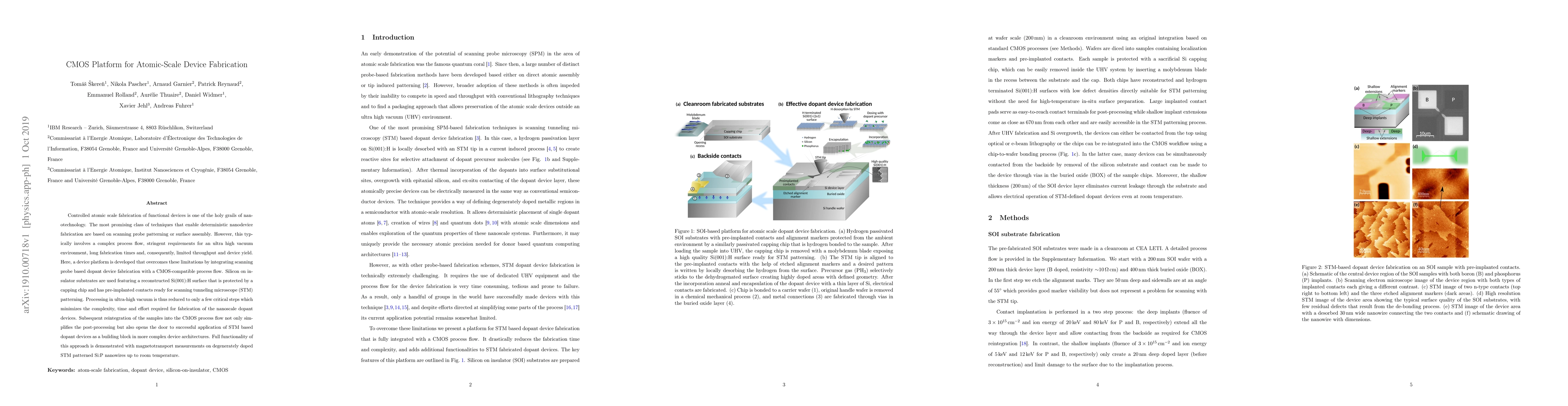
Controlled atomic scale fabrication of functional devices is one of the holy grails of nanotechnology. The most promising class of techniques that enable deterministic nanodevice fabrication are based on scanning probe patterning or surface assembly. However, this typically involves a complex process flow, stringent requirements for an ultra high vacuum environment, long fabrication times and, consequently, limited throughput and device yield. Here, a device platform is developed that overcomes these limitations by integrating scanning probe based dopant device fabrication with a CMOS-compatible process flow. Silicon on insulator substrates are used featuring a reconstructed Si(001):H surface that is protected by a capping chip and has pre-implanted contacts ready for scanning tunneling microscope (STM) patterning. Processing in ultra-high vacuum is thus reduced to only a few critical steps which minimizes the complexity, time and effort required for fabrication of the nanoscale dopant devices. Subsequent reintegration of the samples into the CMOS process flow not only simplifies the post-processing but also opens the door to successful application of STM based dopant devices as a building block in more complex device architectures. Full functionality of this approach is demonstrated with magnetotransport measurements on degenerately doped STM patterned Si:P nanowires up to room temperature.
Get AI-generated insights about this paper's methodology, results, and significance.
Current paper (gray), citations (green), references (blue)
Renhe Chen, Xufeng Kou, Xin Luo et al.
Dries Van Thourhout, Joris Van Campenhout, Didit Yudistira et al.
Title | Authors | Year | Actions |
---|---|---|---|
Direct integration of atomic precision advanced manufacturing into middle-of-line silicon fabrication
|
E. M. Anderson, C. Allemang, A. Leenheer, S. Schmucker, J. Ivie, D. M. Campbell, W. Lepkowski, X. Gao, P. Lu, C. Arose, T.-M. Lu, C. Halsey, T. D. England, D. R. Ward, D. Scrymgeour, S. Misra
|
2025
|
View Paper |
Exploring transport mechanisms in atomic precision advanced manufacturing enabled pn junctions
|
Juan P. Mendez, Xujiao Gao, J. Ivie, James H. G. Owen, Wiley P. Kirk, John N. Randall, Shashank Misra
|
2024
|
View Paper |
DNA-based doping and fabrication of PN diodes
|
Ruobing Bai, Yihan Liu, Bomin Zhang, Beishan Chen, Feng Xiong, Haitao Liu
|
2024
|
View Paper |
Quantifying the Variation in the Number of Donors in Quantum Dots Created Using Atomic Precision Advanced Manufacturing
|
Q. Campbell, J. Koepke, J. Ivie, Andrew M. Mounce, D. Ward, M. Carroll, S. Misra, Andrew D. Baczewski, E. Bussmann
|
2023
|
View Paper |
Suppression of Midinfrared Plasma Resonance Due to Quantum Confinement in
δ
-Doped Silicon
|
S. Young, A. Katzenmeyer, E. Anderson, T. Luk, J. Ivie, S. Schmucker, Xujiao Gao, S. Misra
|
2022
|
View Paper |
Conductivity and size quantization effects in semiconductor \documentclass[12pt]{minimal} \usepackage{amsmath} \usepackage{wasysym} \usepackage{amsfonts} \usepackage{amssymb} \usepackage{amsbsy} \usepackage{mathrsfs} \usepackage{upgreek} \setlength{\oddsidemargin}{-69pt} \begin{document}$$\delta$$\e
|
J. P. Mendez, D. Mamaluy
|
2022
|
View Paper |
Robust incorporation in multi-donor patches created using atomic-precision advanced manufacturing
|
Q. Campbell, J. Koepke, J. Ivie, Andrew M. Mounce, D. Ward, M. Carroll, S. Misra, Andrew D. Baczewski, E. Bussmann
|
2022
|
View Paper |
Current Paths in an Atomic Precision Advanced Manufactured Device Imaged by Nitrogen Vacancy Diamond Magnetic Microscopy.
|
L. Basso, P. Kehayias, J. Henshaw, M. S. Ziabari, H. Byeon, M. Lilly, E. Bussmann, Deanna Campbell, S. Misra, A. Mounce
|
2022
|
View Paper |
Accelerated Lifetime Testing and Analysis of Delta-Doped Silicon Test Structures
|
Connor Halsey, J. Depoy, Deanna Campbell, D. Ward, E. Anderson, S. Schmucker, J. Ivie, Xujiao Gao, D. Scrymgeour, S. Misra
|
2021
|
View Paper |
Revealing quantum effects in highly conductive δ-layer systems
|
D. Mamaluy, J. P. Mendez, Xujiao Gao, S. Misra
|
2021
|
View Paper |
Revealing quantum effects in highly conductive δ-layer systems
|
D. Mamaluy, J. P. Mendez, Xujiao Gao, S. Misra
|
2021
|
View Paper |
Impact of Incorporation Kinetics on Device Fabrication with Atomic Precision
|
J. Ivie, Q. Campbell, J. Koepke, M. Brickson, P. Schultz, R. Muller, Andrew M. Mounce, D. Ward, M. Carroll, E. Bussmann, A. Baczewski, S. Misra
|
2021
|
View Paper |
Fermionic duality: General symmetry of open systems with strong dissipation and memory
|
Valentin Bruch, K. Nestmann, J. Schulenborg, M. Wegewijs
|
2021
|
View Paper |
A Model for Atomic Precision p-Type Doping with Diborane on Si(100)-2×1
|
Q. Campbell, J. Ivie, E. Bussmann, S. Schmucker, Andrew D. Baczewski, S. Misra
|
2020
|
View Paper |
Assessing atomically thin delta-doping of silicon using mid-infrared ellipsometry
|
A. Katzenmeyer, T. Luk, E. Bussmann, S. Young, E. Anderson, M. Marshall, J. A. Ohlhausen, P. Kotula, P. Lu, Deanna Campbell, T. Lu, P. Liu, D. Ward, S. Misra
|
2020
|
View Paper |
Photothermal alternative to device fabrication using atomic precision advanced manufacturing techniques
|
A. Katzenmeyer, Sanja Dmitrovic, A. Baczewski, Q. Campbell, E. Bussmann, T. Lu, E. Anderson, S. Schmucker, J. Ivie, Deanna Campbell, D. Ward, D. Scrymgeour, George T. Wang, S. Misra
|
2020
|
View Paper |
Growth angle-dependent evolution of morphology and magnetic properties of Co films on highly ordered self-organized Ge substrates
|
S. A. Mollick, R. Singh, B. Satpati, S. Bhattacharyya, T. Som
|
2020
|
View Paper |
Mechanism of atomic and close-to-atomic scale cutting of monocrystalline copper
|
W. Xie, F. Fang
|
2020
|
View Paper |
Atomic Precision Advanced Manufacturing for Digital Electronics
|
D. Ward, S. Schmucker, E. Anderson, E. Bussmann, L. Tracy, T. Lu, L. Maurer, Andrew D. Baczewski, Deanna Campbell, M. Marshall, S. Misra
|
2020
|
View Paper |
Observation and origin of the
Δ
manifold in Si:P
δ
layers
|
A. J. Holt, S. Mahatha, R. Stan, F. Strand, T. Nyborg, Davide Curcio, A. Schenk, S. Cooil, M. Bianchi, J. Wells, P. Hofmann, J. Miwa
|
2019
|
View Paper |
Atomic‐Scale Manipulation and In Situ Characterization with Scanning Tunneling Microscopy
|
Wonhee Ko, Chuanxu Ma, G. Nguyen, M. Kolmer, An‐Ping Li
|
2019
|
View Paper |
Comments (0)