Publication
Metrics
AI Quick Summary
Researchers dispute a study claiming quasi-one-dimensional metal-insulator transitions occur in compound semiconductor surfaces through density-functional theory calculations, instead finding an antiferromagnetic ground state with no CDW phase.
Paper Preview
Abstract
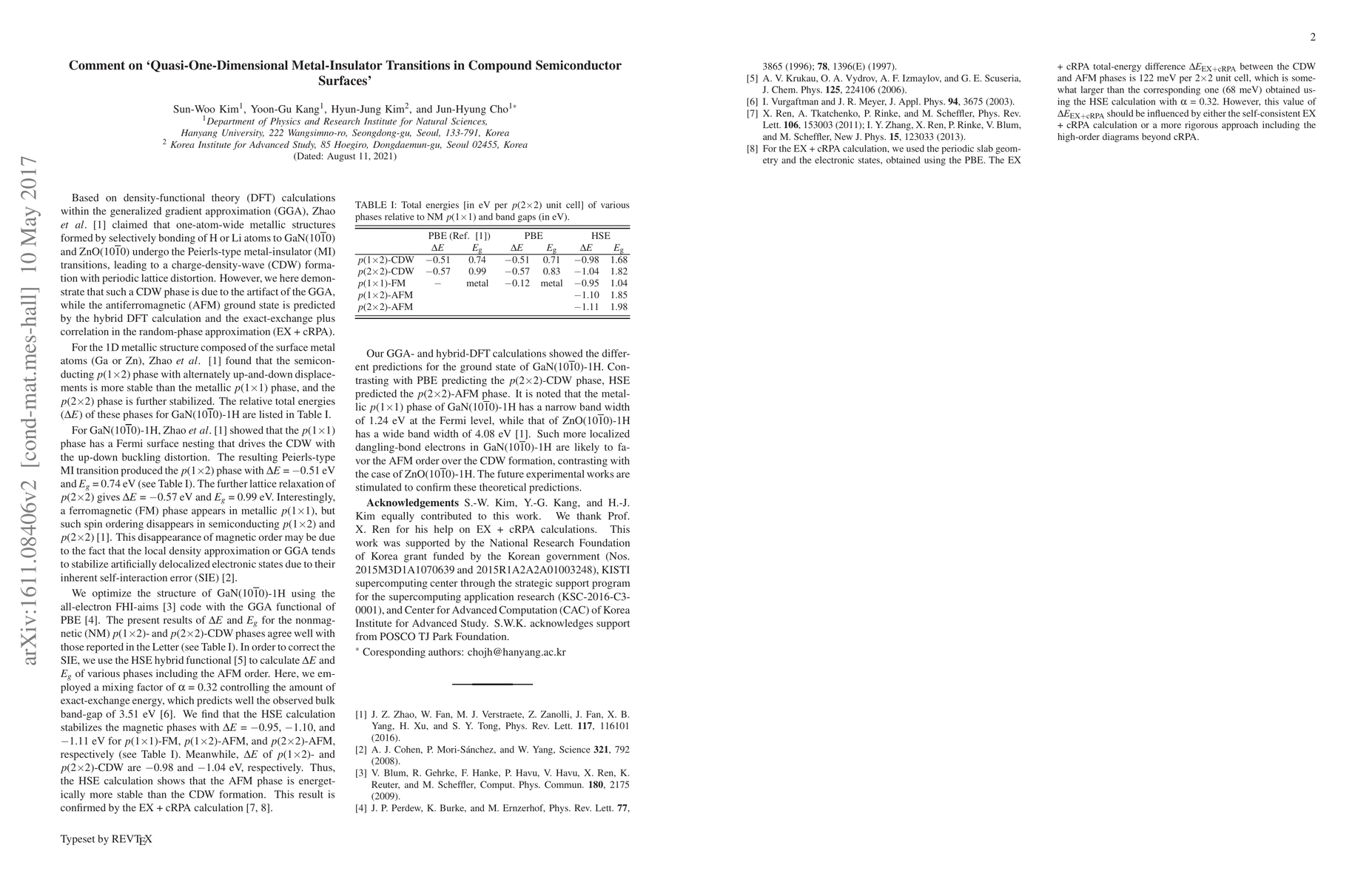
In a recent Letter, Zhao et al. [1] reported the origin of quasi-one-dimensional metal-insulator (MI) transitions in compound semiconductor surfaces. Based on a density-functional theory (DFT) calculation within the generalized gradient approximation (GGA), they claimed that one-atom-wide metallic structures formed by a selective bonding of H or Li atoms to GaN(10-10) and ZnO(10-10) undergo the Peierls-type MI transitions, leading to a charge-density-wave (CDW) formation with periodic lattice distortion. However, we here demonstrate that such a CDW phase is due to the artifact of the GGA, while the antiferromagnetic (AFM) ground state is predicted by the hybrid DFT calculation and the exact-exchange plus correlation in the random-phase approximation (EX + cRPA). [1] J. Z. Zhao, W. Fan, M. J. Verstraete, Z. Zanolli, J. Fan, X. B. Yang, H. Xu, and S. Y. Tong, Phys. Rev. Lett. 117, 116101 (2016).
AI Key Findings
Get AI-generated insights about this paper's methodology, results, significance, and more — seven facets brought into focus.
Impact
Paper Details
PDF Preview
Key Terms
Citation Network
Current paper (gray), citations (green), references (blue)
Display is limited for performance on very large graphs.
Discussion 0