Conduction through subsurface cracks in bulk topological insulators
Publication
Metrics
Paper Preview
Abstract
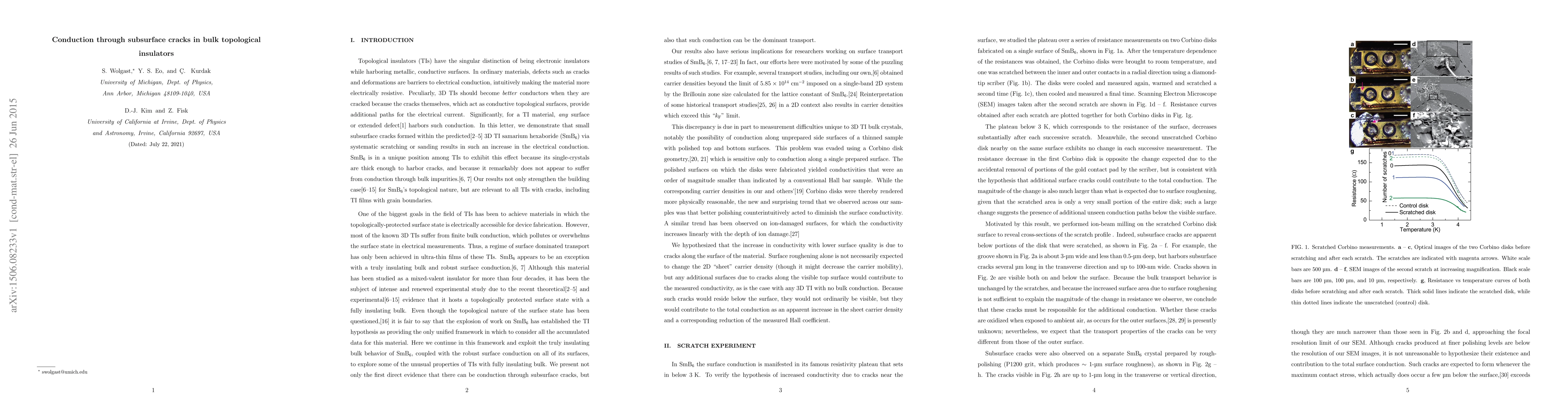
Topological insulators (TIs) have the singular distinction of being electronic insulators while harboring metallic, conductive surfaces. In ordinary materials, defects such as cracks and deformations are barriers to electrical conduction, intuitively making the material more electrically resistive. Peculiarly, 3D TIs should become better conductors when they are cracked because the cracks themselves, which act as conductive topological surfaces, provide additional paths for the electrical current. Significantly, for a TI material, any surface or extended defect harbors such conduction. In this letter, we demonstrate that small subsurface cracks formed within the predicted 3D TI samarium hexaboride (SmB$_{6}$) via systematic scratching or sanding results in such an increase in the electrical conduction. SmB$_{6}$ is in a unique position among TIs to exhibit this effect because its single-crystals are thick enough to harbor cracks, and because it remarkably does not appear to suffer from conduction through bulk impurities. Our results not only strengthen the building case for SmB$_{6}$'s topological nature, but are relevant to all TIs with cracks, including TI films with grain boundaries.
AI Key Findings
Get AI-generated insights about this paper's methodology, results, significance, and more — seven facets brought into focus.
Impact
Paper Details
PDF Preview
Key Terms
Citation Network
Current paper (gray), citations (green), references (blue)
Display is limited for performance on very large graphs.
Discussion 0