Confocal laser scanning microscopy: A tool for rapid optical characterization of 2D materials
Publication
Metrics
AI Quick Summary
Confocal laser scanning microscopy (CLSM) provides a rapid, non-destructive method for analyzing 2D materials like graphene, offering enhanced optical contrast and thickness mapping. CLSM effectively characterizes graphene on various substrates, correlating well with other microscopy techniques while significantly reducing analysis time.
Paper Preview
Abstract
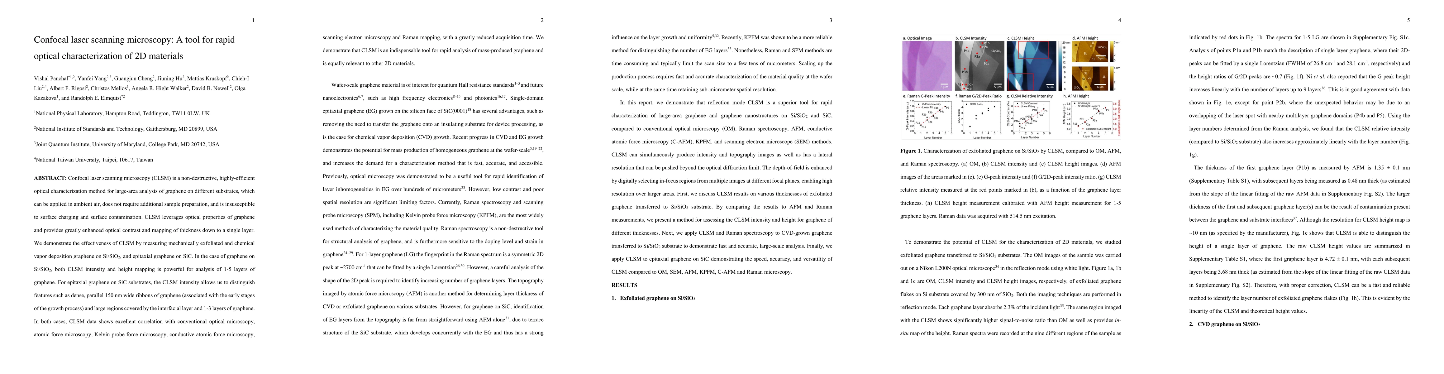
Confocal laser scanning microscopy (CLSM) is a non-destructive, highly-efficient optical characterization method for large-area analysis of graphene on different substrates, which can be applied in ambient air, does not require additional sample preparation, and is insusceptible to surface charging and surface contamination. CLSM leverages optical properties of graphene and provides greatly enhanced optical contrast and mapping of thickness down to a single layer. We demonstrate the effectiveness of CLSM by measuring mechanically exfoliated and chemical vapor deposition graphene on Si/SiO2, and epitaxial graphene on SiC. In the case of graphene on Si/SiO2, both CLSM intensity and height mapping is powerful for analysis of 1-5 layers of graphene. For epitaxial graphene on SiC substrates, the CLSM intensity allows us to distinguish features such as dense, parallel 150 nm wide ribbons of graphene (associated with the early stages of the growth process) and large regions covered by the interfacial layer and 1-3 layers of graphene. In both cases, CLSM data shows excellent correlation with conventional optical microscopy, atomic force microscopy, Kelvin probe force microscopy, conductive atomic force microscopy, scanning electron microscopy and Raman mapping, with a greatly reduced acquisition time. We demonstrate that CLSM is an indispensable tool for rapid analysis of mass-produced graphene and is equally relevant to other 2D materials.
AI Key Findings
Get AI-generated insights about this paper's methodology, results, significance, and more — seven facets brought into focus.
Impact
Paper Details
PDF Preview
Key Terms
Citation Network
Current paper (gray), citations (green), references (blue)
Display is limited for performance on very large graphs.
Discussion 0