Publication
Metrics
AI Quick Summary
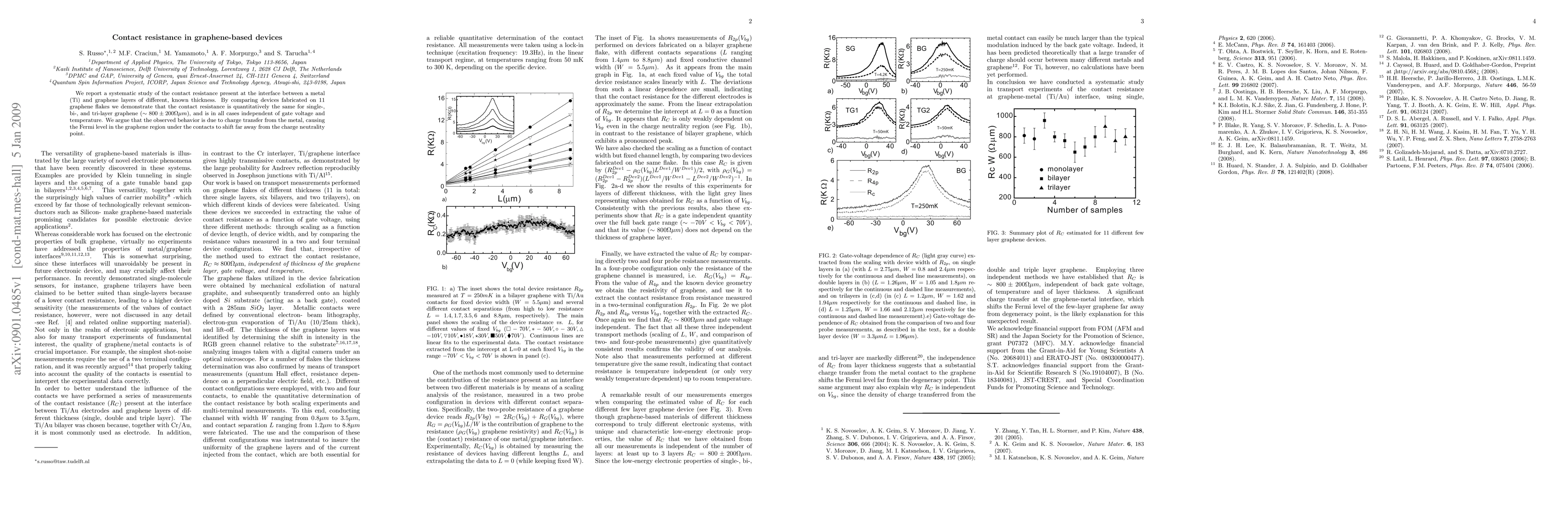
This study reveals consistent contact resistance ($\sim800 \pm 200 \Omega \mu m$) between titanium and graphene layers, regardless of graphene thickness or environmental conditions, attributing this behavior to charge transfer shifting the Fermi level away from neutrality.
Paper Preview
Abstract
We report a systematic study of the contact resistance present at the interface between a metal (Ti) and graphene layers of different, known thickness. By comparing devices fabricated on 11 graphene flakes we demonstrate that the contact resistance is quantitatively the same for single-, bi-, and tri-layer graphene ($\sim800 \pm 200 \Omega \mu m$), and is in all cases independent of gate voltage and temperature. We argue that the observed behavior is due to charge transfer from the metal, causing the Fermi level in the graphene region under the contacts to shift far away from the charge neutrality point.
AI Key Findings
Get AI-generated insights about this paper's methodology, results, significance, and more — seven facets brought into focus.
Impact
Paper Details
PDF Preview
Key Terms
Citation Network
Current paper (gray), citations (green), references (blue)
Display is limited for performance on very large graphs.
Discussion 0