ArxivLens

Quick Summary:

This research demonstrates how controllable phase transitions between multiple charge density wave (CDW) phases in monolayer 1T-VSe$_2$ can be achieved via doping and strain engineering. First-principles calculations reveal that the ground state of VSe$_2$ can transition from a $\sqrt7 \times \sqrt3$ CDW to $3 \times \sqrt3$ and $4\times 4$ phases through doping and compressive strain, suggesting VSe$_2$ as a promising material for tunable electronic devices.

DOI: 10.1063/5.0068241
arXiv Id: 2011.03692
Date Published: 2021-11-03
Date Updated: 2021-11-03

Categories:

Key Terms (TF-IDF):

cdw (0.380)
_2 (0.265)
monolayer (0.260)
doping (0.248)
times (0.209)
bulk (0.193)
strain (0.189)
unit (0.159)
transitions (0.156)
formula (0.151)
phase (0.150)
charge (0.140)
compressive (0.125)
stabilized (0.124)
density wave (0.123)
controllable (0.123)
charge density (0.121)
starting point (0.121)
concentrations (0.119)
phase transitions (0.114)
License: http://arxiv.org/licenses/nonexclusive-distrib/1.0/

Summary:

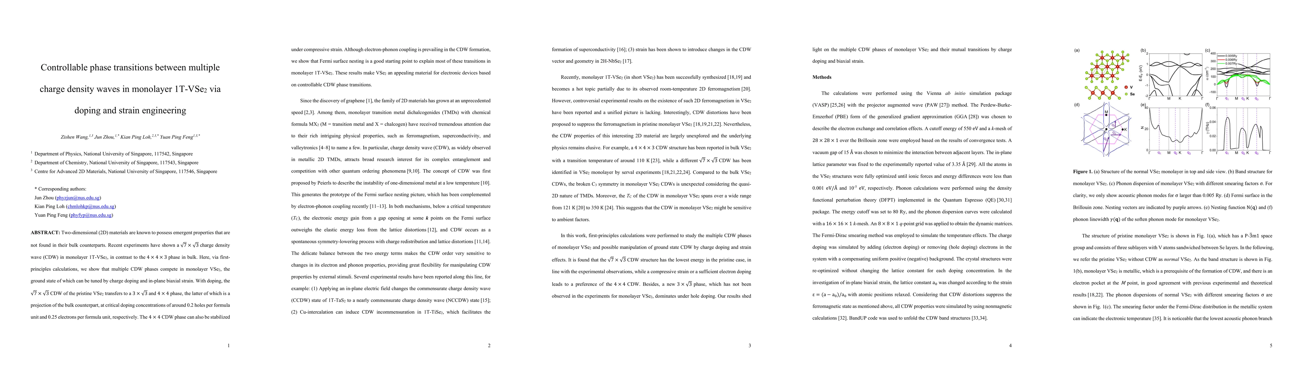
Two-dimensional (2D) materials are known to possess emergent properties that are not found in their bulk counterparts. Recent experiments have shown a $\sqrt7 \times \sqrt3$ charge density wave (CDW) in monolayer 1T-VSe$_2$, in contrast to the $4\times 4\times 3$ phase in bulk. Here, via first-principles calculations, we show that multiple CDW phases compete in monolayer VSe$_2$, the ground state of which can be tuned by charge doping and in-plane biaxial strain. With doping, the $\sqrt7 \times \sqrt3$ CDW of the pristine VSe$_2$ transfers to a $3 \times \sqrt3$ and $4\times 4$ phase, the latter of which is a projection of the bulk counterpart, at critical doping concentrations of around 0.2 holes per formula unit and 0.25 electrons per formula unit, respectively. The $4\times 4$ CDW phase can also be stabilized under compressive strain. Although electron-phonon coupling is prevailing in the CDW formation, we show that Fermi surface nesting is a good starting point to explain most of these transitions in monolayer 1T-VSe$_2$. These results make VSe$_2$ an appealing material for electronic devices based on controllable CDW phase transitions.

Citation & Reference Network Visualization

This graph shows how this paper is connected to other research. The current paper is shown in dark gray, papers that cite it are in green, and papers it references are in blue. You can:

Current Paper
Papers citing this work (Citations)
Papers cited by this work (References)

• Hover over any node to see the paper title

• Click a node to view that paper's details

• Drag nodes to rearrange the graph

• Use the zoom controls (bottom right) to zoom in/out

Citations and References

Title Authors Year Actions
Unveiling the microscopic dynamics of the charge density wave transition in monolayer <mml:math xmlns:mml="http://www.w3.org/1998/Math/MathML"><mml:mrow><mml:mi mathvariant="normal">V</mml:mi><mml:msub><mml:mi>X</mml:mi><mml:mn>2</mml:mn></mml:msub></mml:mrow></mml:math> ( <mml:math xmlns:mml="htt
Yuxuan Chen, Chao Liang, Jian Yuan, Biao Wang, Huashan Li
2024
View Paper
Interplay of the charge density wave transition with topological and superconducting properties.
Zishen Wang, J. You, Chuan Chen, Jinchao Mo, Jingyu He, Lishu Zhang, Jun Zhou, K. Loh, Yuanping Feng
2023
View Paper
Coexistence of ferromagnetism and charge density waves in monolayer LaBr2.
Jun Zhou, Zishen Wang, Shijie Wang, Yuanping Feng, Ming Yang, L. Shen
2023
View Paper
2D Vanadium Sulfides: Synthesis, Atomic Structure Engineering, and Charge Density Waves
Camiel van Efferen, Joshua Hall, N. Atodiresei, V. Boix, Affan Safeer, Tobias Wekking, Nikolay A Vinogradov, Alexei B Preobrajenski, Jan Knudsen, J. Fischer, Wouter Jolie, T. Michely
2023
View Paper
Formation of Monolayer Charge Density Waves and Anomalous Edge Doping in Na Doped Bulk VSe2
Ulysse Chazarin, Mahé Lezoualc'h, J. Chou, W. Pai, A. Karn, R. Sankar, Cyril Chacon, Y. Girard, V. Repain, A. Bellec, S. Rousset, A. Smogunov, Y. Dappe, J. Lagoute
2022
View Paper
Emergent Topological Superconductor by Charge Density Wave Transition
Zishen Wang, J. You, Chuan Chen, Jinchao Mo, Jingyu He, Lishu Zhang, Jun Zhou, K. Loh, Y. Feng
2022
View Paper
Probing the Origin of Chiral Charge Density Waves in the Two-Dimensional Limits.
Ziying Wang, Zishen Wang, Y. Feng, K. Loh
2022
View Paper
Decisive role of electron-phonon coupling for phonon and electron instabilities in transition metal dichalcogenides
Zishen Wang, Chuan Chen, Jinchao Mo, Jun Zhou, K. Loh, Y. Feng
2022
View Paper
Hole doping dependent electronic instability and electron-phonon coupling in infinite-layer nickelates
Xuelei Sui, Jianfeng Wang, Chao Chen, Xiangui Ding, K. Zhou, C. Cao, L. Qiao, Haiqing Lin, Bing Huang
2022
View Paper
Novel 2D vanadium sulphides: synthesis, atomic structure engineering and charge density waves
Camiel van Efferen, Joshua Hall, V. Boix, Tobias Wekking, N. Vinogradov, Alexei Preobrajensk, J. Knudsen, J. Fischer, Wouter Jolie, T. Michely
2023
View Paper

Similar Papers

A combined Quantum Monte Carlo and DFT study of the strain response and magnetic properties of two-dimensional (2D) 1T-VSe$_2$ with charge density wave

Sergiy Krylyuk, Kamal Choudhary, Li Yin, Albert Davydov, Daniel Wines, Jaron T. Krogel, Kayahan Saritas, Can Ataca, Angela R. Hight Walker, Aubrey T. Hanbicki, Adam L. Friedman, Francesca Tavazza, Brian Donovan, Tom Berlijn, Akram Ibrahim, Gregory M. Stephen, Nishwanth Gudibandla, Tehseen Adel, Frank M. Abel, Sharadh Jois, Michelle E. Jamer

Published: 2024-09-27

Comments (0)

This website uses cookies to ensure you get the best experience. Learn more