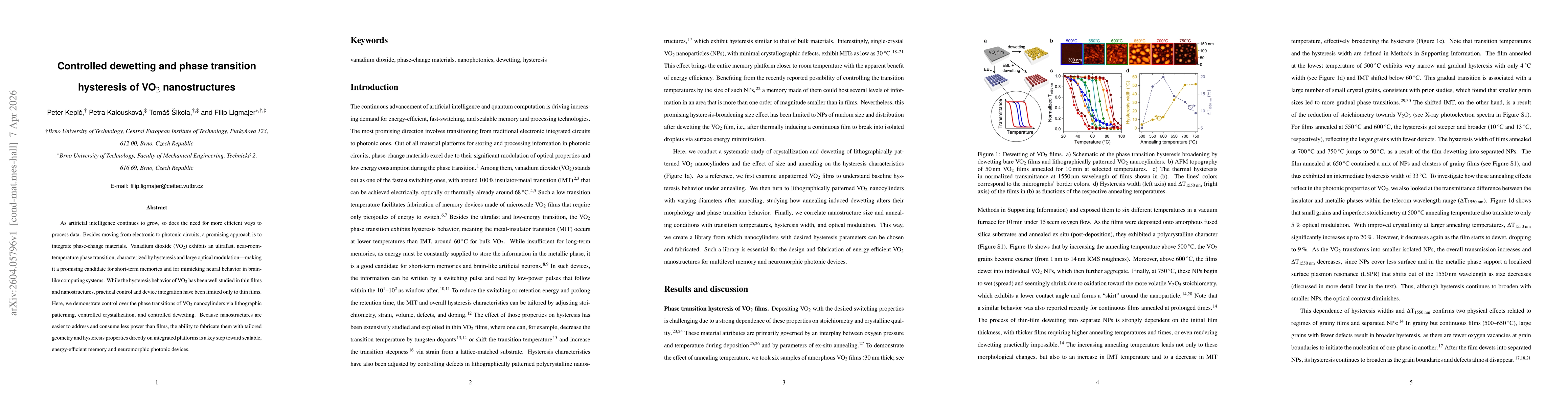
Lithographically patterned VO2 nanocylinders were annealed in oxygen at 500–750 °C to induce controlled crystallization and dewetting, followed by AFM/SEM imaging and infrared transmission measurements at 1550 nm to assess hysteresis and optical modulation.
Controlled dewetting and phase transition hysteresis of VO2 nanostructures
Publication
Metrics
Quick Answers
What methodology did the authors use?
Lithographically patterned VO2 nanocylinders were annealed in oxygen at 500–750 °C to induce controlled crystallization and dewetting, followed by AFM/SEM imaging and infrared transmission measurements at 1550 nm to assess hysteresis and optical modulation. More in Methodology →
What are the key results?
Deterministic dewetting window at 700 °C: cylinders ≤400 nm collapse into a single ~220 nm nanoparticle; — Vertical volume growth up to 2× during crystallization, grain coarsening up to 600 °C, and dewetting above 600 °C; More in Key Results →
Why is this work significant?
The study provides a scalable route to engineer VO2 nanostructures with tailored phase‑transition hysteresis and optical contrast, essential for compact, energy‑efficient neuromorphic photonic memories and logic. More in Significance →
What are the main limitations?
Global annealing crystallizes all features simultaneously, limiting individual tuning; — Post‑dewetting nanoparticle size shows significant variability, affecting reproducibility. More in Limitations →
Abstract
As artificial intelligence continues to grow, so does the need for more efficient ways to process data. Besides moving from electronic to photonic circuits, a promising approach is to integrate phase-change materials. Vanadium dioxide (VO$_2$) exhibits an ultrafast, near-room-temperature phase transition, characterized by hysteresis and large optical modulation -- making it a promising candidate for short-term memories and for mimicking neural behavior in brain-like computing systems. While the hysteresis behavior of VO$_2$ has been well studied in thin films and nanostructures, practical control and device integration have been limited only to thin films. Here, we demonstrate control over the phase transitions of VO$_2$ nanocylinders via lithographic patterning, controlled crystallization, and controlled dewetting. Because nanostructures are easier to address and consume less power than films, the ability to fabricate them with tailored geometry and hysteresis properties directly on integrated platforms is a key step toward scalable, energy-efficient memory and neuromorphic photonic devices.
Key Findings, in focus
Seven facets of this paper, analysed and brought into focus by AI.
The study provides a scalable route to engineer VO2 nanostructures with tailored phase‑transition hysteresis and optical contrast, essential for compact, energy‑efficient neuromorphic photonic memories and logic.
- Deterministic dewetting window at 700 °C: cylinders ≤400 nm collapse into a single ~220 nm nanoparticle;
- Vertical volume growth up to 2× during crystallization, grain coarsening up to 600 °C, and dewetting above 600 °C;
- Size‑dependent hysteresis width decreases exponentially with cylinder diameter, enabling tunable memory states, and LSPR‑enhanced optical modulation for 400–600 nm diameters.
The study provides a scalable route to engineer VO2 nanostructures with tailored phase‑transition hysteresis and optical contrast, essential for compact, energy‑efficient neuromorphic photonic memories and logic.
A systematic mapping of annealing‑induced morphological evolution to phase‑transition hysteresis in lithographically defined VO2 nanostructures, demonstrating deterministic dewetting and size‑dependent hysteresis control.
First demonstration of controlled dewetting and hysteresis tuning in VO2 nanostructures, combining lithographic patterning, annealing, and optical characterization to create a library of tunable photonic memory building blocks.
- Global annealing crystallizes all features simultaneously, limiting individual tuning;
- Post‑dewetting nanoparticle size shows significant variability, affecting reproducibility.
- Implement local selective crystallization (laser or spatial‑light modulation) to achieve single‑particle tuning;
- Integrate the engineered nanostructures into on‑chip photonic circuits and evaluate device performance.
Discussion 0