Publication
Metrics
AI Quick Summary
Researchers developed a method to precisely control the thickness of oxide layers on 2D molybdenum disulfide (MoTe2) flakes using ozone exposure, with potential applications in metal-oxide-semiconductor technology.
Paper Preview
Abstract
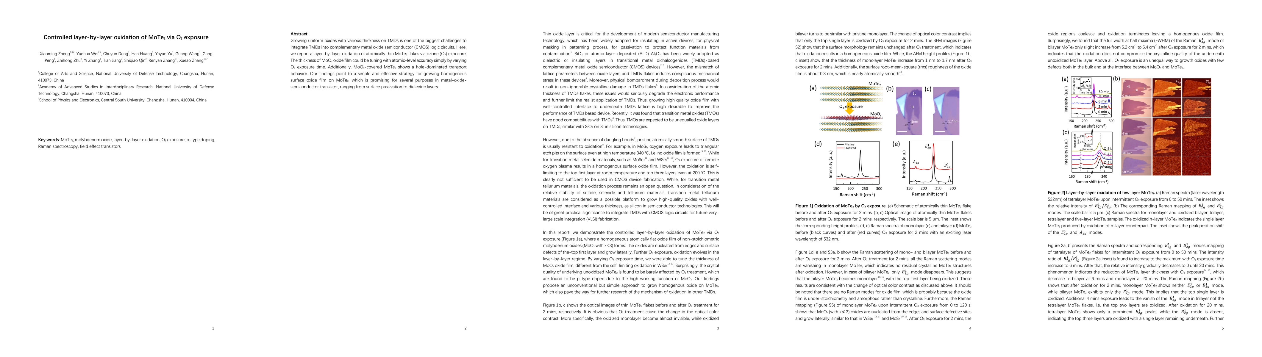
Growing uniform oxides with various thickness on TMDs is one of the biggest challenges to integrate TMDs into complementary metal oxide semiconductor (CMOS) logic circuits. Here, we report a layer-by-layer oxidation of atomically thin MoTe2 flakes via ozone (O3) exposure. The thickness of MoOx oxide film could be tuning with atomic-level accuracy simply by varying O3 exposure time. Additionally, MoOx-covered MoTe2 shows a hole-dominated transport behavior. Our findings point to a simple and effective strategy for growing homogenous surface oxide film on MoTe2, which is promising for several purposes in metal-oxide-semiconductor transistor, ranging from surface passivation to dielectric layers.
AI Key Findings
Get AI-generated insights about this paper's methodology, results, significance, and more — seven facets brought into focus.
Impact
Paper Details
PDF Preview
Key Terms
Citation Network
Current paper (gray), citations (green), references (blue)
Display is limited for performance on very large graphs.
Discussion 0