Publication
Metrics
AI Quick Summary
This research explores hybrid superconductor-semiconductor heterostructures using InAs quantum wells, demonstrating that surface morphology and growth temperature significantly affect electron mobility. By capping with In$_{0.81}$Al$_{0.19}$As, the Fermi level pinning is controlled, with calculations confirming pinning positions at \SI{40}{\milli eV} and \SI{309}{\milli eV} above the Fermi level.
Paper Preview
Abstract
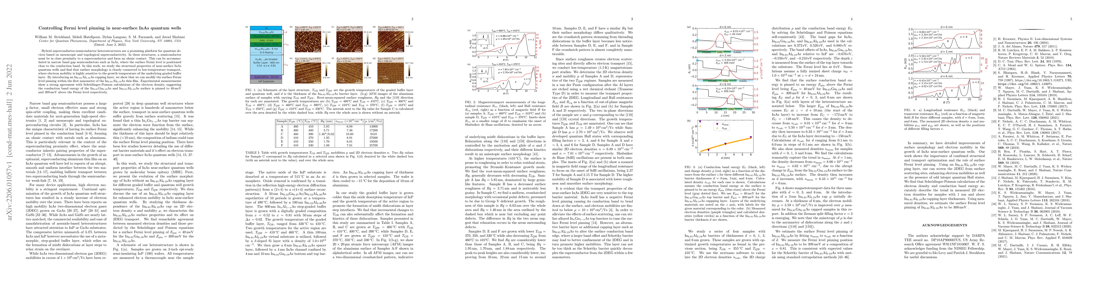
Hybrid superconductor-semiconductor heterostructures are a promising platform for quantum devices based on mesoscopic and topological superconductivity. In these structures, a semiconductor must be in close proximity to a superconductor and form an ohmic contact. This can be accommodated in narrow band gap semiconductors such as InAs, where the surface Fermi level is positioned close to the conduction band. In this work, we study the structural properties of near-surface InAs quantum wells and find that surface morphology is closely connected to low-temperature transport, where electron mobility is highly sensitive to the growth temperature of the underlying graded buffer layer. By introducing an In$_{0.81}$Al$_{0.19}$As capping layer, we show that we can modify the surface Fermi level pinning within the first nanometer of the In$_{0.81}$Al$_{0.19}$As thin film. Experimental measurements show a strong agreement with Schr\"odinger-Poisson calculations of the electron density, suggesting the conduction band energy of the In$_{0.81}$Ga$_{0.19}$As and In$_{0.81}$Al$_{0.19}$As surface is pinned to \SI{40}{\milli eV} and \SI{309}{\milli eV} above the Fermi level respectively.
AI Key Findings
Get AI-generated insights about this paper's methodology, results, significance, and more — seven facets brought into focus.
Impact
Paper Details
Authors
PDF Preview
Key Terms
Citation Network
Current paper (gray), citations (green), references (blue)
Display is limited for performance on very large graphs.
Discussion 0