Copper Thin Film Deposition by An Indigenous Unbalanced Type DC Magnetron Sputtering System
Publication
Metrics
AI Quick Summary
This study investigates the deposition of copper thin films using an indigenous unbalanced type DC magnetron sputtering system on glass and silicon substrates. The research focuses on the crystalline structure and crystallite grain size of the deposited copper, which is crucial for its applications in photo-catalytic and sensor technologies. Characterization is performed using X-Ray Fluorescence and X-Ray Diffraction techniques.
Paper Preview
Abstract
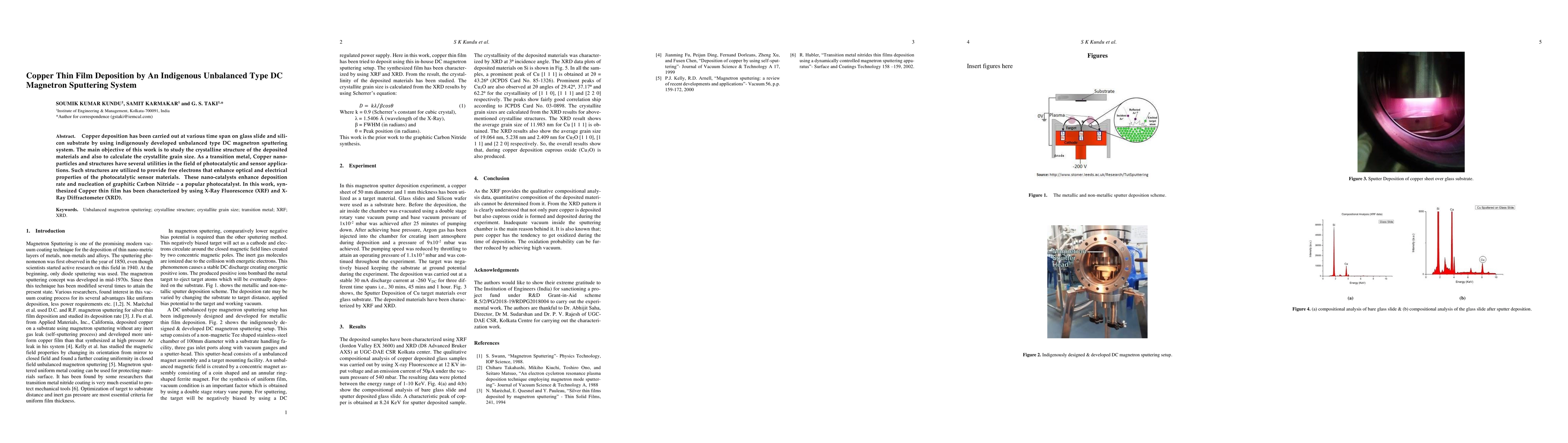
Copper deposition has been carried out at various time span on glass slide and silicon substrate by using indigenously developed unbalanced type DC magnetron sputtering system. The main objective of this work is to study the crystalline structure of the deposited materials and also to calculate the crystallite grain size. As a transition metal, Copper nano-particles and structures have several utilities in the field of photo-catalytic and sensor applications. Such structures are utilized to provide free electrons that enhance optical and electrical properties of the photo-catalytic sensor mate-rials. These nano-catalysts enhance deposition rate and nucleation of graphitic Carbon Nitride, a popular photo-catalyst. In this work, synthesized Copper thin film has been characterized by using X-Ray Fluorescence and X-Ray Diffractometer.
AI Key Findings
Get AI-generated insights about this paper's methodology, results, significance, and more — seven facets brought into focus.
Impact
Paper Details
Authors
PDF Preview
Key Terms
Citation Network
Current paper (gray), citations (green), references (blue)
Display is limited for performance on very large graphs.
Discussion 0