This paper demonstrates the efficient coupling of a quantum emitter in hexagonal boron nitride (hBN), a 2D material, with a tapered optical fiber, achieving a collection efficiency of 10%. The study also analyzes the angular emission pattern and shows the potential for fully integrated photonic circuits.
Realization of integrated photonic circuits on a single chip requires controlled manipulation and integration of solid-state quantum emitters with nanophotonic components. Previous works focused on emitters embedded in a three-dimensional crystals -- such as nanodiamonds or quantum dots. In contrast, in this work we demonstrate coupling of a single emitter in a two-dimensional (2D) material, namely hexagonal boron nitride (hBN), with a tapered optical fiber and find a collection efficiency of the system is found to be 10~\%. Furthermore, due to the single dipole character of the emitter, we were able to analyse the angular emission pattern of the coupled system via back focal plane imaging. The good coupling efficiency to the tapered fiber even allows excitation and detection in a fully fiber coupled way yielding a true integrated system. Our results provide evidence of the feasibility to efficiently integrate quantum emitters in 2D materials with photonic structures.
Generated Sep 03, 2025
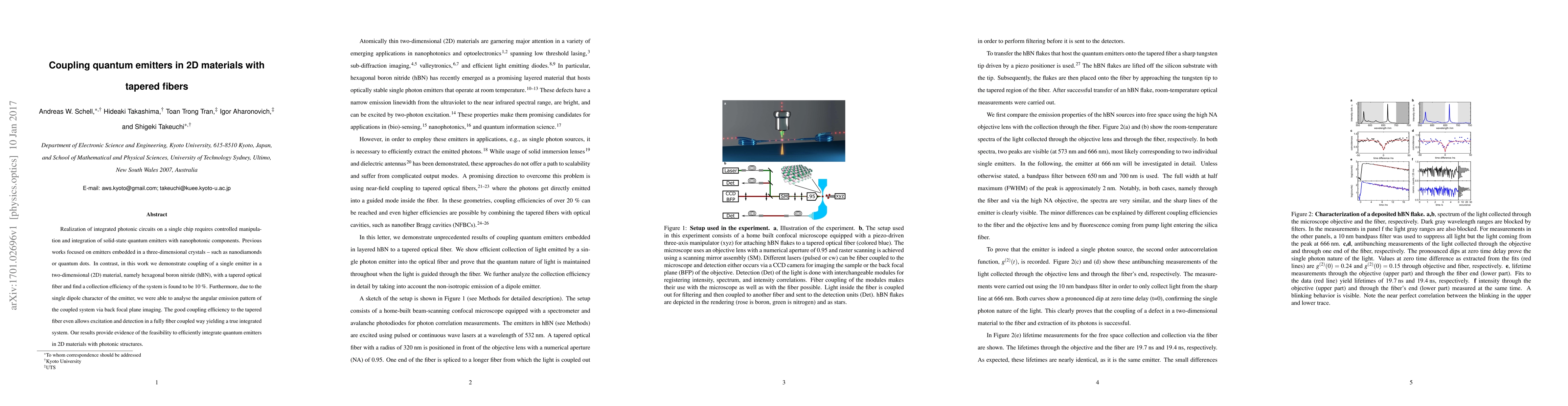
The research utilized a homebuilt confocal microscope setup with a sharp tungsten tip and a three-axis piezo stage. The microscope objective used has a numerical aperture of 0.95, and scanning is achieved via a scanning mirror unit. Excitation lasers at 532 nm wavelength are provided by a continuous wave laser and a picosecond laser. Detection is done via avalanche photodiodes or a Peltier-cooled camera behind a monochromator. Back focal plane imaging is performed using a Peltier-cooled camera.
This research is significant as it demonstrates a method for integrating quantum emitters in 2D materials with photonic structures, which is crucial for realizing integrated photonic circuits on a single chip. The findings pave the way for promising applications in integrated quantum photonics using single emitters in hBN.
The paper presents a novel approach to couple a single quantum emitter in a 2D material (hBN) with a tapered optical fiber, demonstrating high collection efficiency and integrated system capabilities.
This work distinguishes itself by focusing on 2D materials like hBN instead of the previously studied three-dimensional crystals, and by successfully demonstrating efficient coupling with a tapered fiber for both excitation and detection.
Current paper (gray), citations (green), references (blue)
Display is limited for performance on very large graphs.
Galan Moody, Kamyar Parto, Shaimaa I. Azzam
Title | Authors | Year | Actions |
---|
Comments (0)