Publication
Metrics
AI Quick Summary
This research demonstrates the efficient coupling of single photon emitters in WSe2 monolayers to surface plasmons guided by metal-insulator-metal waveguides, achieving an average enhancement in emission rate by a factor of 1.89, paving the way for on-chip quantum photonics.
Paper Preview
Abstract
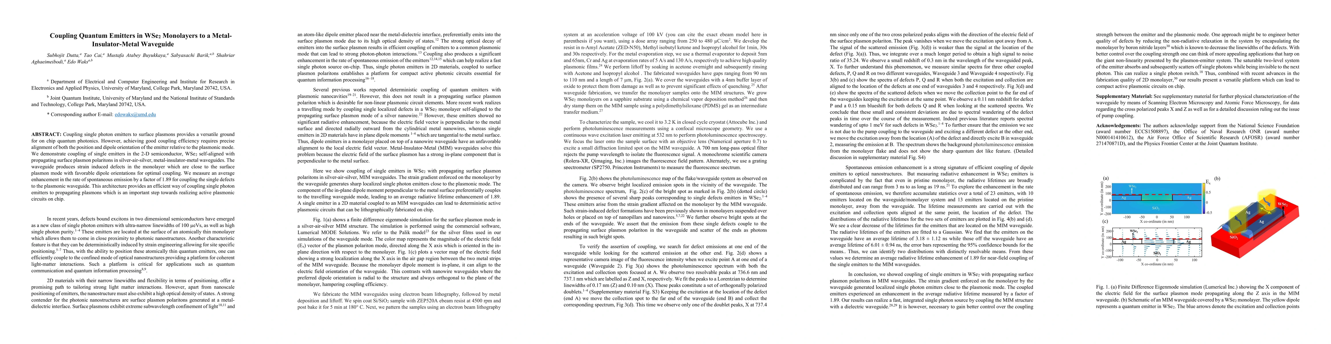
Coupling single photon emitters to surface plasmons provides a versatile ground for on chip quantum photonics. However, achieving good coupling efficiency requires precise alignment of both the position and dipole orientation of the emitter relative to the plasmonic mode. We demonstrate coupling of single emitters in the 2-D semiconductor, WSe2 self-aligned with propagating surface plasmon polaritons in silver-air-silver, metal-insulator-metal waveguides. The waveguide produces strain induced defects in the monolayer which are close to the surface plasmon mode with favorable dipole orientations for optimal coupling. We measure an average enhancement in the rate of spontaneous emission by a factor of 1.89 for coupling the single defects to the plasmonic waveguide. This architecture provides an efficient way of coupling single photon emitters to propagating plasmons which is an important step towards realizing active plasmonic circuits on chip.
AI Key Findings
Get AI-generated insights about this paper's methodology, results, significance, and more — seven facets brought into focus.
Impact
Paper Details
PDF Preview
Key Terms
Citation Network
Current paper (gray), citations (green), references (blue)
Display is limited for performance on very large graphs.
Discussion 0