Cryogenic packaging of nanophotonic devices with a low coupling loss < 1 dB
Publication
Metrics
AI Quick Summary
This paper presents a method for cryogenically packaging nanophotonic devices, achieving record-low coupling losses of <1 dB at near-infrared wavelengths and maintaining stability from room to ultra-low temperatures. The technique enables scalable integration of photonic technologies for quantum and classical applications.
Paper Preview
Abstract
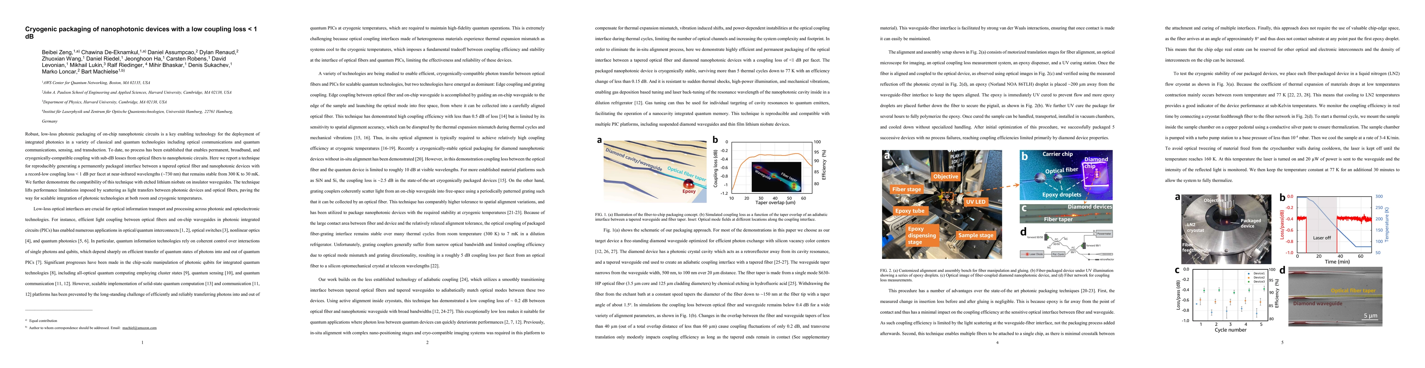
Robust, low-loss photonic packaging of on-chip nanophotonic circuits is a key enabling technology for the deployment of integrated photonics in a variety of classical and quantum technologies including optical communications and quantum communications, sensing, and transduction. To date, no process has been established that enables permanent, broadband, and cryogenically-compatible coupling with sub-dB losses from optical fibers to nanophotonic circuits. Here we report a technique for reproducibly generating a permanently packaged interface between a tapered optical fiber and nanophotonic devices with a record-low coupling loss < 1 dB per facet at near-infrared wavelengths (~730 nm) that remains stable from 300 K to 30 mK. We further demonstrate the compatibility of this technique with etched lithium niobate on insulator waveguides. The technique lifts performance limitations imposed by scattering as light transfers between photonic devices and optical fibers, paving the way for scalable integration of photonic technologies at both room and cryogenic temperatures.
AI Key Findings
Get AI-generated insights about this paper's methodology, results, significance, and more — seven facets brought into focus.
Impact
Paper Details
Authors
PDF Preview
Key Terms
Citation Network
Current paper (gray), citations (green), references (blue)
Display is limited for performance on very large graphs.
Discussion 0