Current-Mode Deep Level Transient Spectroscopy of a Semiconductor Nanowire Field-Effect Transistor
Publication
Metrics
AI Quick Summary
This paper introduces current-mode deep-level transient spectroscopy (I-DLTS) to analyze deep trap levels in semiconductor nanowires, overcoming the limitations of traditional DLTS. The technique measures the temperature-dependent transient current in response to gate voltage pulses, demonstrating its effectiveness in determining defect states and surface barrier heights in zinc oxide nanowires.
Paper Preview
Abstract
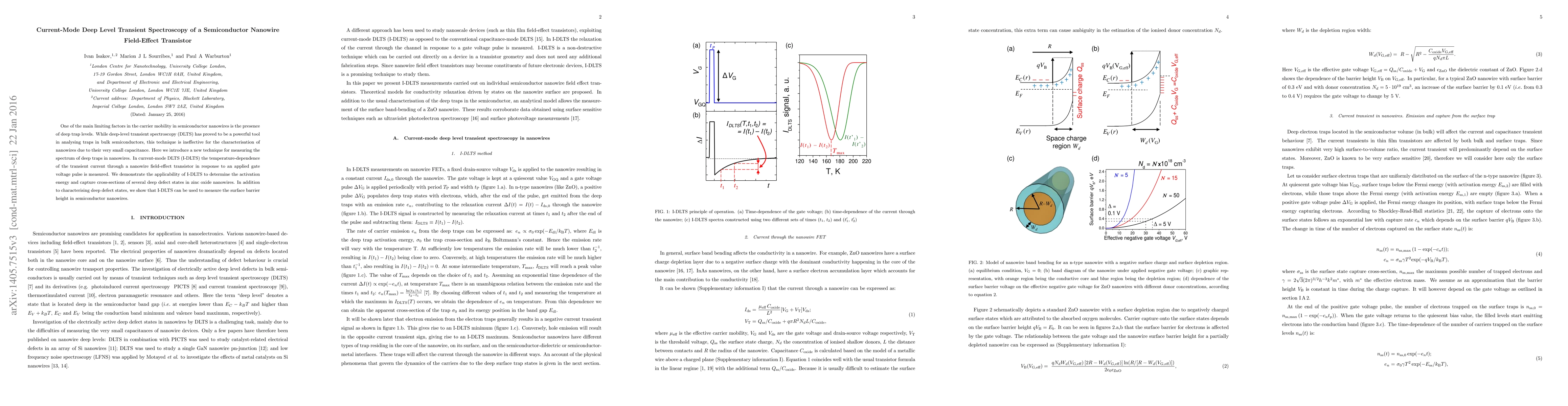
One of the main limiting factors in the carrier mobility in semiconductor nanowires is the presence of deep trap levels. While deep-level transient spectroscopy (DLTS) has proved to be a powerful tool in analysing traps in bulk semiconductors, this technique is ineffective for the characterisation of nanowires due to their very small capacitance. Here we introduce a new technique for measuring the spectrum of deep traps in nanowires. In current-mode DLTS (I-DLTS) the temperature-dependence of the transient current through a nanowire field-effect transistor in response to an applied gate voltage pulse is measured. We demonstrate the applicability of I-DLTS to determine the activation energy and capture cross-sections of several deep defect states in zinc oxide nanowires. In addition to characterising deep defect states, we show that I-DLTS can be used to measure the surface barrier height in semiconductor nanowires.
AI Key Findings
Get AI-generated insights about this paper's methodology, results, significance, and more — seven facets brought into focus.
Impact
Paper Details
PDF Preview
Key Terms
Citation Network
Current paper (gray), citations (green), references (blue)
Display is limited for performance on very large graphs.
Discussion 0