Publication
Metrics
AI Quick Summary
This study investigates the removal of individual halogen atoms from Cl- and Br-terminated Si(100) surfaces using scanning tunneling microscopy, revealing three charge states of resulting silicon dangling bonds. Density functional theory and STM findings suggest the charge states can be manipulated to locally adjust surface reactivity.
Paper Preview
Abstract
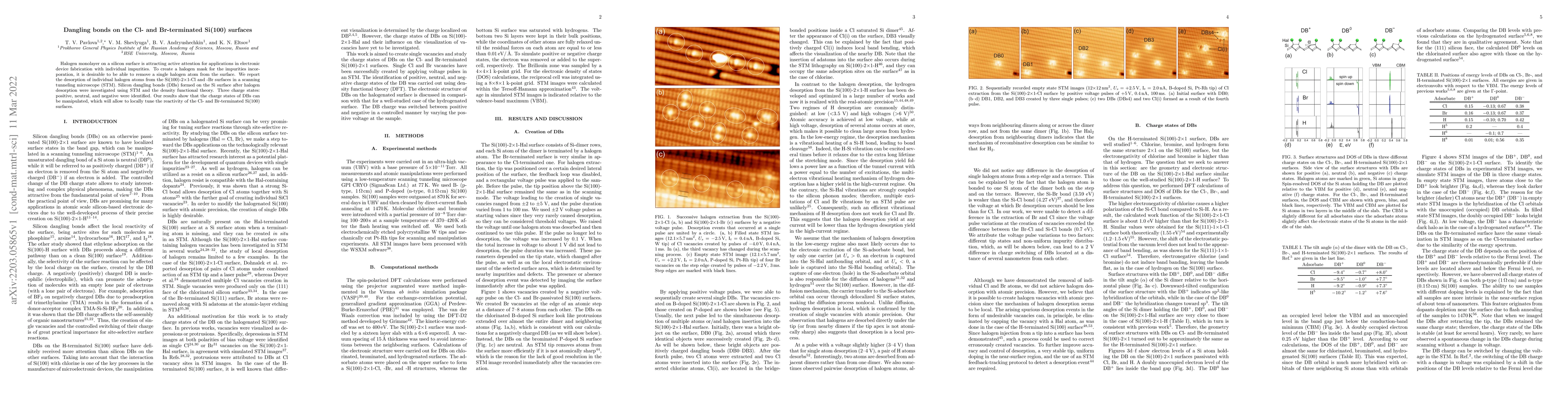
Halogen monolayer on a silicon surface is attracting active attention for applications in electronic device fabrication with individual impurities. To create a halogen mask for the impurities incorporation, it is desirable to be able to remove a single halogen atom from the surface. We report the desorption of individual halogen atoms from the Si(100)-2x1-Cl and -Br surfaces in a scanning tunneling microscope (STM). Silicon dangling bonds (DBs) formed on the Si surface after halogen desorption were investigated using STM and the density functional theory. Three charge states: positive, neutral, and negative were identified. Our results show that the charge states of DBs can be manipulated, which will allow to locally tune the reactivity of the Cl- and Br-terminated Si(100) surfaces.
AI Key Findings — Failed
Key findings generation failed. Failed to start generation process
Impact
Paper Details
Authors
PDF Preview
Key Terms
Citation Network
Current paper (gray), citations (green), references (blue)
Display is limited for performance on very large graphs.
Discussion 0