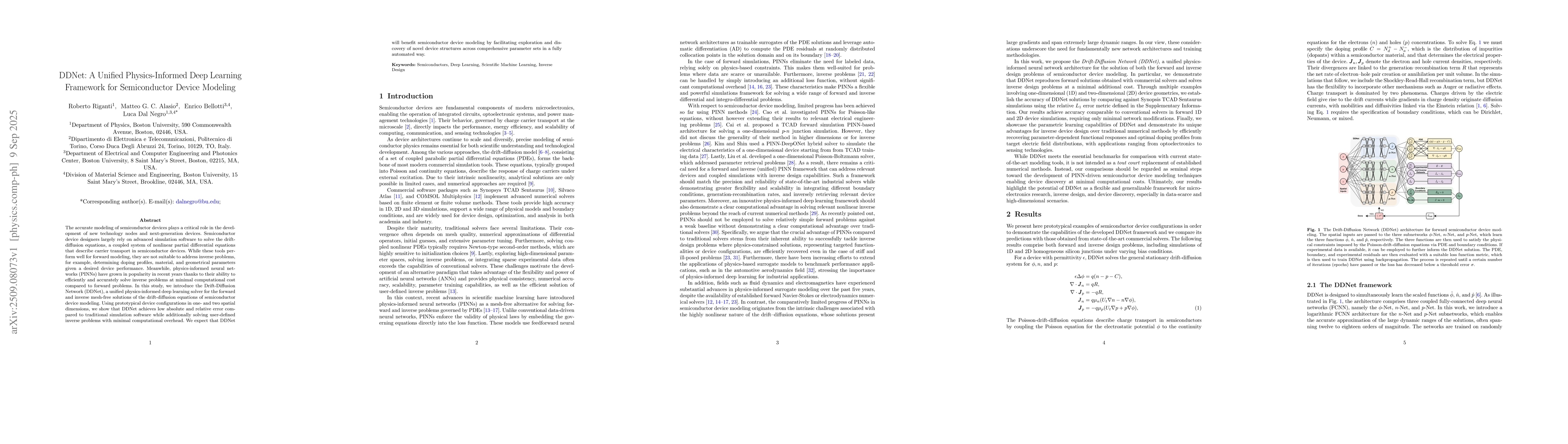
The accurate modeling of semiconductor devices plays a critical role in the
development of new technology nodes and next-generation devices. Semiconductor
device designers largely rely on advanced simulation software to solve the
drift-diffusion equations, a coupled system of nonlinear partial differential
equations that describe carrier transport in semiconductor devices. While these
tools perform well for forward modeling, they are not suitable to address
inverse problems, for example, determining doping profiles, material, and
geometrical parameters given a desired device performance. Meanwhile,
physics-informed neural networks (PINNs) have grown in popularity in recent
years thanks to their ability to efficiently and accurately solve inverse
problems at minimal computational cost compared to forward problems. In this
study, we introduce the Drift-Diffusion Network (DDNet), a unified
physics-informed deep learning solver for the forward and inverse mesh-free
solutions of the drift-diffusion equations of semiconductor device modeling.
Using prototypical device configurations in one- and two spatial dimensions, we
show that DDNet achieves low absolute and relative error compared to
traditional simulation software while additionally solving user-defined inverse
problems with minimal computational overhead. We expect that DDNet will benefit
semiconductor device modeling by facilitating exploration and discovery of
novel device structures across comprehensive parameter sets in a fully
automated way.
Discussion 0