Deep Learning-based Multi Project InP Wafer Simulation for Unsupervised Surface Defect Detection
Publication
Metrics
AI Quick Summary
Researchers developed a deep learning-based method to generate synthetic golden standards for surface defect detection in Indium-Phosphide wafer manufacturing, outperforming traditional decision-tree approaches.
Paper Preview
Abstract
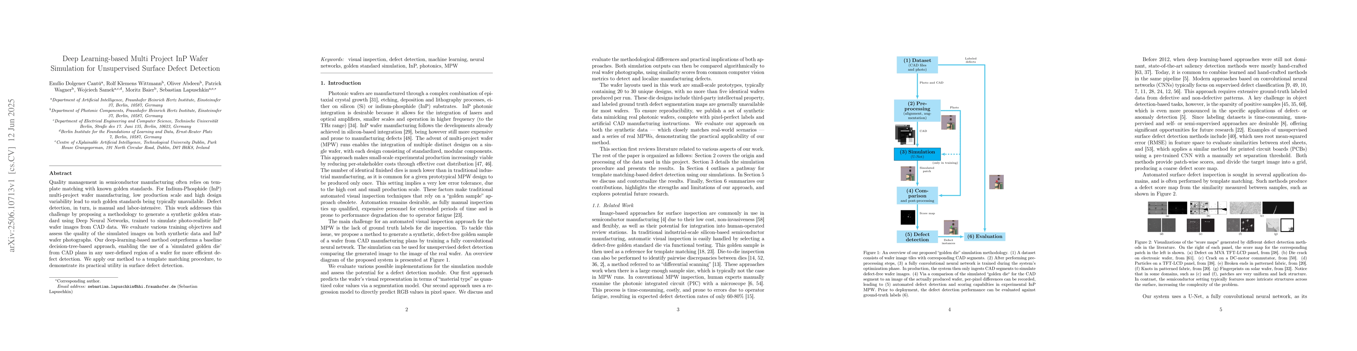
Quality management in semiconductor manufacturing often relies on template matching with known golden standards. For Indium-Phosphide (InP) multi-project wafer manufacturing, low production scale and high design variability lead to such golden standards being typically unavailable. Defect detection, in turn, is manual and labor-intensive. This work addresses this challenge by proposing a methodology to generate a synthetic golden standard using Deep Neural Networks, trained to simulate photo-realistic InP wafer images from CAD data. We evaluate various training objectives and assess the quality of the simulated images on both synthetic data and InP wafer photographs. Our deep-learning-based method outperforms a baseline decision-tree-based approach, enabling the use of a 'simulated golden die' from CAD plans in any user-defined region of a wafer for more efficient defect detection. We apply our method to a template matching procedure, to demonstrate its practical utility in surface defect detection.
AI Key Findings
Get AI-generated insights about this paper's methodology, results, significance, and more — seven facets brought into focus.
Authors
PDF Preview
Related Papers
No references found for this paper.
Discussion 0