Deep Learning Regression of VLSI Plasma Etch Metrology
Publication
Metrics
Paper Preview
Abstract
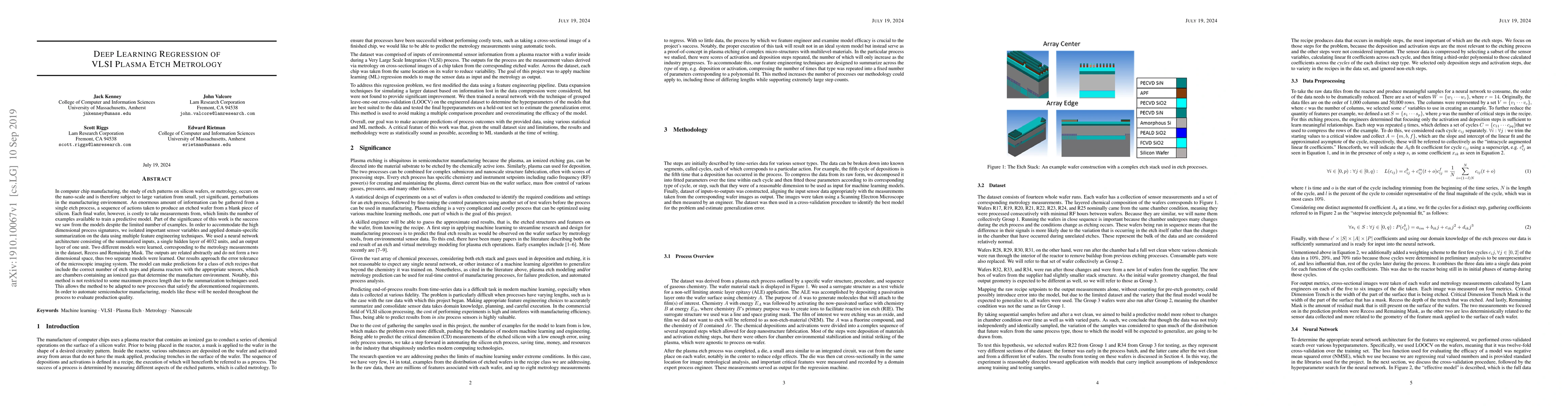
In computer chip manufacturing, the study of etch patterns on silicon wafers, or metrology, occurs on the nano-scale and is therefore subject to large variation from small, yet significant, perturbations in the manufacturing environment. An enormous amount of information can be gathered from a single etch process, a sequence of actions taken to produce an etched wafer from a blank piece of silicon. Each final wafer, however, is costly to take measurements from, which limits the number of examples available to train a predictive model. Part of the significance of this work is the success we saw from the models despite the limited number of examples. In order to accommodate the high dimensional process signatures, we isolated important sensor variables and applied domain-specific summarization on the data using multiple feature engineering techniques. We used a neural network architecture consisting of the summarized inputs, a single hidden layer of 4032 units, and an output layer of one unit. Two different models were learned, corresponding to the metrology measurements in the dataset, Recess and Remaining Mask. The outputs are related abstractly and do not form a two dimensional space, thus two separate models were learned. Our results approach the error tolerance of the microscopic imaging system. The model can make predictions for a class of etch recipes that include the correct number of etch steps and plasma reactors with the appropriate sensors, which are chambers containing an ionized gas that determine the manufacture environment. Notably, this method is not restricted to some maximum process length due to the summarization techniques used. This allows the method to be adapted to new processes that satisfy the aforementioned requirements. In order to automate semiconductor manufacturing, models like these will be needed throughout the process to evaluate production quality.
AI Key Findings
Get AI-generated insights about this paper's methodology, results, significance, and more — seven facets brought into focus.
Impact
Paper Details
Authors
PDF Preview
Key Terms
Citation Network
Current paper (gray), citations (green), references (blue)
Display is limited for performance on very large graphs.
Discussion 0