01
MethodologyHow they did it
A combination of experimental and theoretical methods were used to study the properties of ZnIn2S4 flakes.
This paper investigates the impact of Zn-In anti-structural defects on the electronic structure and optical properties of few-layer hexagonal ZnIn2S4. The study reveals that these defects create donor and acceptor levels, leading to tunable defect emission and in-plane dipole orientation, which can be manipulated via electrostatic gating for advanced optoelectronic applications.
This paper investigates the impact of Zn-In anti-structural defects on the electronic structure and optical properties of few-layer hexagonal ZnIn2S4. The study reveals that these defects create donor and acceptor levels, leading to tunable defect emission and in-plane dipole orientation, which can be manipulated via electrostatic gating for advanced optoelectronic applications.
A combination of experimental and theoretical methods were used to study the properties of ZnIn2S4 flakes. More in Methodology →
The bandgap of ZnIn2S4 flakes was determined to be 2.88-2.98 eV. — The optical absorption spectra showed a direct band gap. More in Key Results →
This study provides new insights into the properties of ZnIn2S4 flakes, which has potential applications in optoelectronic devices. More in Significance →
The sample size was limited to 12 layers. — The measurement conditions may not be optimal for all samples. More in Limitations →
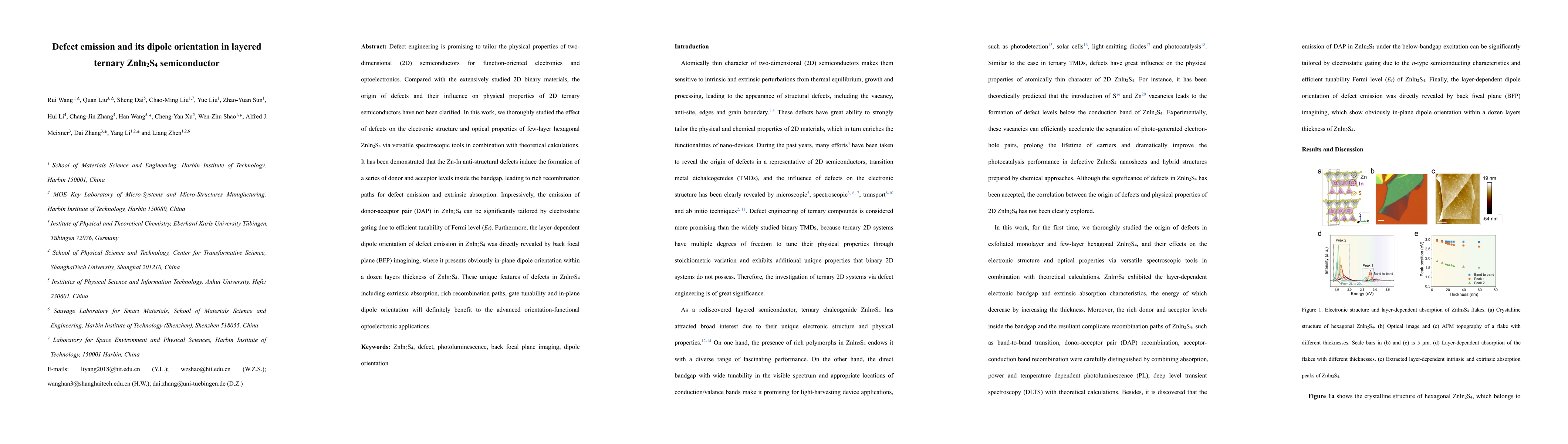
Defect engineering is promising to tailor the physical properties of two-dimensional (2D) semiconductors for function-oriented electronics and optoelectronics. Compared with the extensively studied 2D binary materials, the origin of defects and their influence on physical properties of 2D ternary semiconductors have not been clarified. In this work, we thoroughly studied the effect of defects on the electronic structure and optical properties of few-layer hexagonal Znln2S4 via versatile spectroscopic tools in combination with theoretical calculations. It has been demonstrated that the Zn-In anti-structural defects induce the formation of a series of donor and acceptor levels inside the bandgap, leading to rich recombination paths for defect emission and extrinsic absorption. Impressively, the emission of donor-acceptor pair (DAP) in Znln2S4 can be significantly tailored by electrostatic gating due to efficient tunability of Fermi level (Ef). Furthermore, the layer-dependent dipole orientation of defect emission in Znln2S4 was directly revealed by back focal plane (BFP) imagining, where it presents obviously in-plane dipole orientation within a dozen layers thickness of Znln2S4. These unique features of defects in Znln2S4 including extrinsic absorption, rich recombination paths, gate tunability and in-plane dipole orientation will definitely benefit to the advanced orientation-functional optoelectronic applications.
Seven facets of this paper, analysed and brought into focus by AI.
This study provides new insights into the properties of ZnIn2S4 flakes, which has potential applications in optoelectronic devices.
A combination of experimental and theoretical methods were used to study the properties of ZnIn2S4 flakes.
This study provides new insights into the properties of ZnIn2S4 flakes, which has potential applications in optoelectronic devices.
The study presents a new understanding of the optical and electrical properties of ZnIn2S4 flakes, which is essential for their potential applications.
This work demonstrates the importance of studying the properties of 2D materials in terms of their electronic and optical behavior.
Current paper (gray), citations (green), references (blue)
Display is limited for performance on very large graphs.
Discussion 0