Defect evolution and interplay in n-type InN
Publication
Metrics
AI Quick Summary
Researchers studied n-type InN epilayers using positron annihilation spectroscopy and transmission electron microscopy to investigate defect evolution and interplay. They found that Si-doping led to the formation of vacancy defects at the interface, which affected the film's structure and carrier concentration.
Paper Preview
Abstract
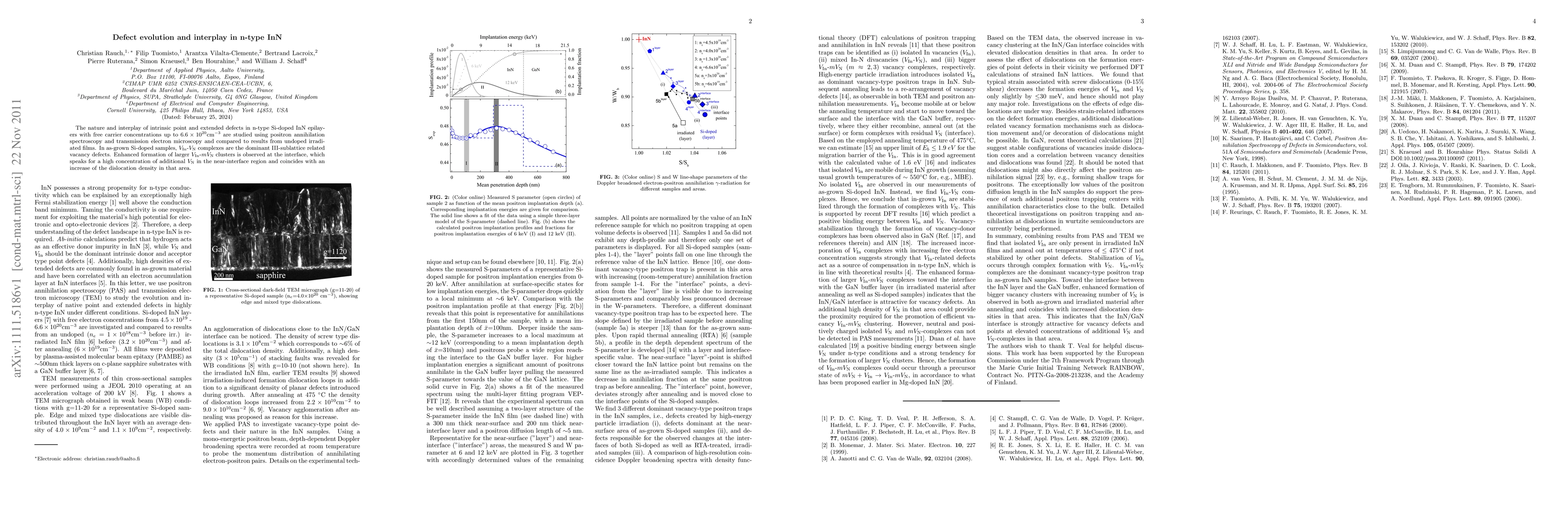
The nature and interplay of intrinsic point and extended defects in n-type Si-doped InN epilayers with free carrier concentrations up to 6.6x10E20cm-3 are studied using positron annihilation spectroscopy and transmission electron microscopy and compared to results from undoped irradiated films. In as-grown Si-doped samples, V_In-V_N complexes are the dominant III-sublattice related vacancy defects. Enhanced formation of larger V_In-mV_N clusters is observed at the interface, which speaks for high concentrations of additional V_N in the near-interface region and coincides with an increase in the density of screw and edge type dislocations in that area.
AI Key Findings
Get AI-generated insights about this paper's methodology, results, significance, and more — seven facets brought into focus.
Impact
Paper Details
PDF Preview
Key Terms
Citation Network
Current paper (gray), citations (green), references (blue)
Display is limited for performance on very large graphs.
Discussion 0