Publication
Metrics
AI Quick Summary
This paper proposes a novel method to simulate steady illumination conditions, demonstrating that defect formation energies remain unaffected by illumination. It introduces a unified framework using an effective temperature and a universal Fermi level to describe electron distributions under steady illumination, revealing that band edge 'defect' states' formation energies shift with electron temperature, influencing defect ionic probabilities and charged defect concentrations. The theory is applied to explain doping behaviors in GaN:Mg and CdTe:Sb, aligning with experimental observations.
Paper Preview
Abstract
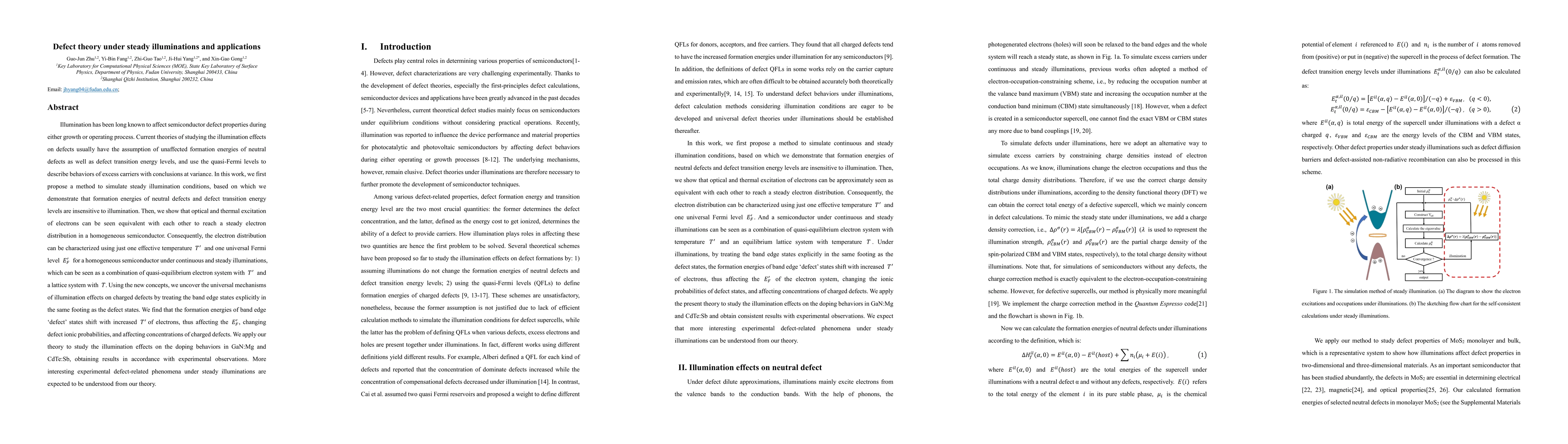
Illumination has been long known to affect semiconductor defect properties during either growth or operating process. Current theories of studying the illumination effects on defects usually have the assumption of unaffected formation energies of neutral defects as well as defect transition energy levels, and use the quasi-Fermi levels to describe behaviors of excess carriers with conclusions at variance. In this work, we first propose a method to simulate steady illumination conditions, based on which we demonstrate that formation energies of neutral defects and defect transition energy levels are insensitive to illumination. Then, we show that optical and thermal excitation of electrons can be seen equivalent with each other to reach a steady electron distribution in a homogeneous semiconductor. Consequently, the electron distribution can be characterized using just one effective temperature T' and one universal Fermi level E_F' for a homogeneous semiconductor under continuous and steady illuminations, which can be seen as a combination of quasi-equilibrium electron system with T' and a lattice system with T. Using the new concepts, we uncover the universal mechanisms of illumination effects on charged defects by treating the band edge states explicitly in the same footing as the defect states. We find that the formation energies of band edge 'defect' states shift with increased T' of electrons, thus affecting the E_F', changing defect ionic probabilities, and affecting concentrations of charged defects. We apply our theory to study the illumination effects on the doping behaviors in GaN:Mg and CdTe:Sb, obtaining results in accordance with experimental observations. More interesting experimental defect-related phenomena under steady illuminations are expected to be understood from our theory.
AI Key Findings
Get AI-generated insights about this paper's methodology, results, significance, and more — seven facets brought into focus.
Impact
Paper Details
Authors
PDF Preview
Key Terms
Citation Network
Current paper (gray), citations (green), references (blue)
Display is limited for performance on very large graphs.
Discussion 0