01
MethodologyHow they did it
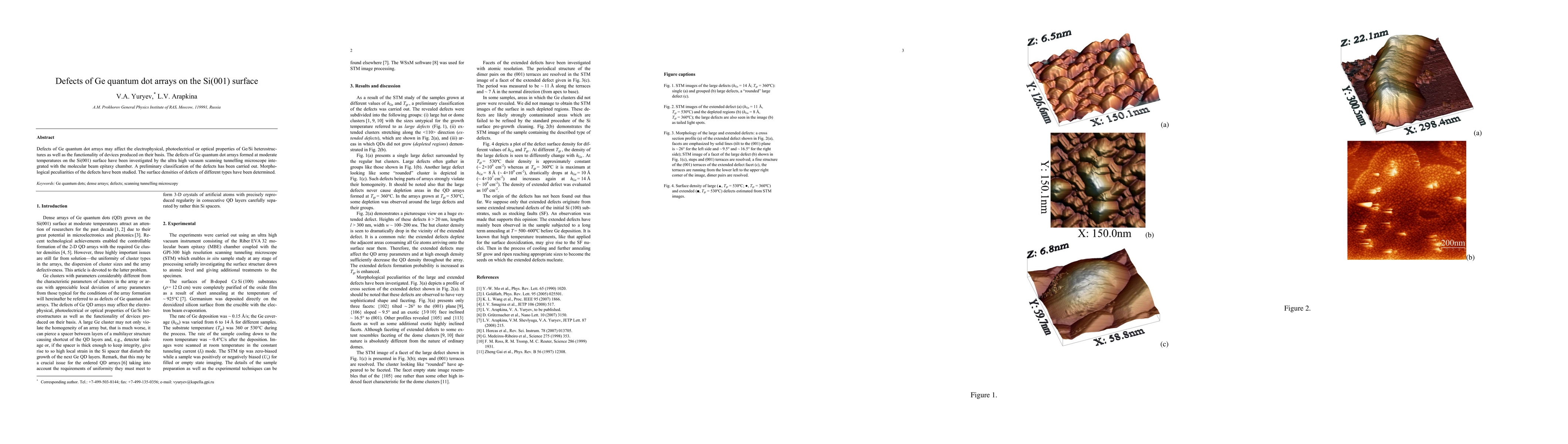
The study investigated defects in Ge quantum dot arrays on Si(001) surface using ultra-high vacuum scanning tunnelling microscopy integrated with a molecular beam epitaxy chamber, processing STM images with WSxM software.
Discussion 0