Summary

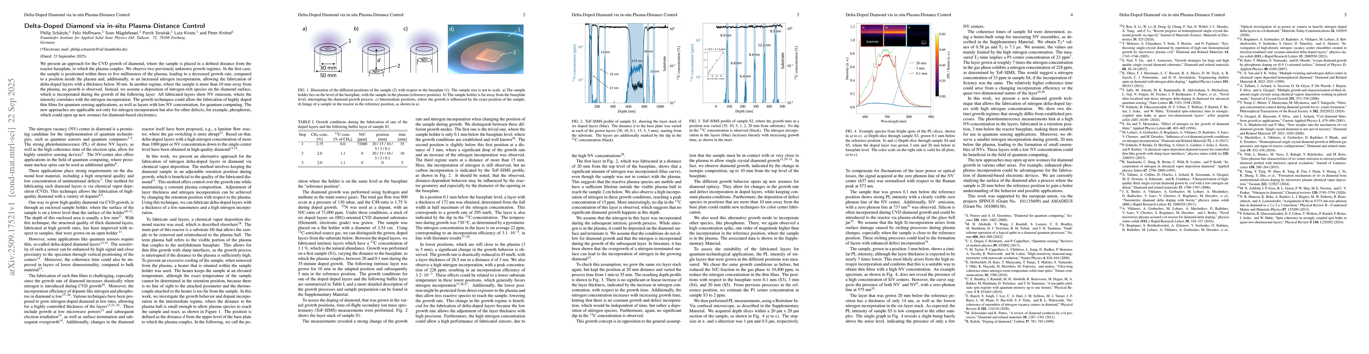
We present an approach for the CVD growth of diamond, where the sample is placed in a defined distance from the reactor baseplate, to which the plasma couples. We observe two previously unknown growth regimes. In the first case, the sample is positioned within three to five millimeters of the plasma, leading to a decreased growth rate, compared to a position inside the plasma and, additionally, to an increased nitrogen incorporation, allowing the fabrication of delta-doped layers with a thickness below 30 nm. In another regime, where the sample is more than 10 mm away from the plasma, no growth is observed. Instead, we assume a deposition of nitrogen-rich species on the diamond surface, which is incorporated during the growth of the following layer. All fabricated layers show NV emission, where the intensity correlates with the nitrogen incorporation. The growth techniques could allow the fabrication of highly doped thin films for quantum sensing applications, as well as layers with low NV concentration, for quantum computing. The new approaches are applicable not only for nitrogen incorporation but also for other defects, for example, phosphorus, which could open up new avenues for diamond-based electronics.

AI Key Findings

Generated Sep 29, 2025

Methodology

The study employs in-situ plasma-distance control during chemical vapor deposition (CVD) to grow diamond layers, varying the sample's position relative to the reactor baseplate to observe growth regimes and nitrogen incorporation effects.

Key Results

  • Two distinct growth regimes were identified: one with reduced growth rate and increased nitrogen incorporation near the plasma (3-5 mm distance), enabling delta-doped layers <30 nm thick, and another with no growth at >10 mm distance.
  • Nitrogen-rich species deposition on diamond surfaces at >10 mm distance leads to nitrogen incorporation during subsequent layer growth, with NV emission intensity correlating to nitrogen concentration.
  • Delta-doped layers with high NV concentration (up to 228 ppm) were fabricated, suitable for quantum sensing, while low NV concentration layers (14 nm thick) were found beneficial for quantum computing.

Significance

This research enables precise control over nitrogen doping in diamond, opening new avenues for quantum technologies like sensing and computing, as well as diamond-based electronics through defect incorporation.

Technical Contribution

Introduces in-situ plasma-distance control during CVD growth to achieve precise defect incorporation and growth rate modulation in diamond layers.

Novelty

Identifies previously unknown growth regimes based on plasma-distance positioning, enabling delta-doping with sub-30 nm thickness and controlled defect incorporation for quantum applications.

Limitations

  • The study primarily focuses on nitrogen doping, with limited exploration of other defect species beyond phosphorus.
  • The exact mechanisms of nitrogen incorporation at >10 mm distance require further investigation.

Future Work

  • Exploring defect incorporation beyond nitrogen, such as phosphorus, for electronic applications.
  • Investigating the surface effects and defect behavior at 20 mm distance to optimize growth conditions.
  • Developing scalable methods for industrial diamond growth with controlled defect incorporation.

Paper Details

PDF Preview

Download PDF

Comments (0)

This website uses cookies to ensure you get the best experience. Learn more