01
MethodologyHow they did it
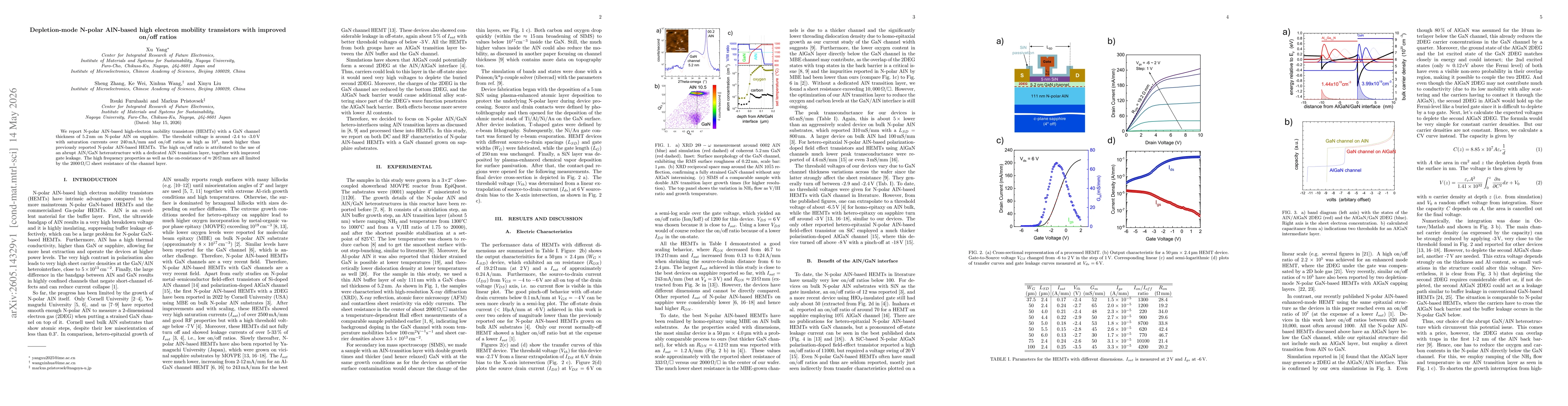
N-polar AlN-based HEMTs with a GaN channel thickness of 5.2 nm were grown on N-polar AlN on sapphire using a close-coupled MOVPE reactor, including an AlN buffer, a dedicated AlN transition layer, and an abrupt AlN/GaN heterostructure; devices were fabricated with Ti/Al/Ni/Au ohmic contacts, Ni/Au gates, and SiN passivation, followed by RF and DC characterization to assess on/off ratio, threshold voltage, Isat, and high-frequency performance.
Discussion 0