Design flow for readout ASICs in High-energy Physics experiments
Publication
Metrics
AI Quick Summary
Researchers developed a mixed-signal design flow for readout ASICs in high-energy physics experiments, enabling faster simulation and reducing functionality mismatches.
Paper Preview
Abstract
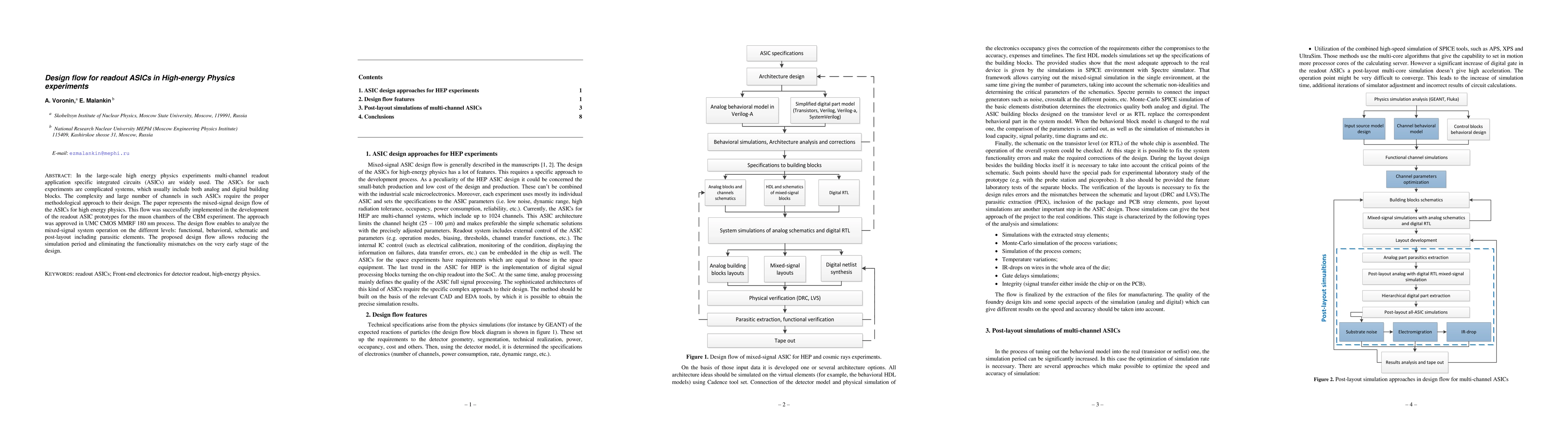
In the large-scale high energy physics experiments multi-channel readout application specific integrated circuits (ASICs) are widely used. The ASICs for such experiments are complicated systems, which usually include both analog and digital building blocks. The complexity and large number of channels in such ASICs require the proper methodological approach to their design. The paper represents the mixed-signal design flow of the ASICs for high energy physics. This flow was successfully implemented in the development of the readout ASIC prototypes for the muon chambers of the CBM experiment. The approach was approved in UMC CMOS MMRF 180 nm process. The design flow enables to analyze the mixed-signal system operation on the different levels: functional, behavioral, schematic and post-layout including parasitic elements. The proposed design flow allows reducing the simulation period and eliminating the functionality mismatches on the very early stage of the design.
AI Key Findings
Get AI-generated insights about this paper's methodology, results, significance, and more — seven facets brought into focus.
Impact
Paper Details
PDF Preview
Key Terms
Citation Network
Current paper (gray), citations (green), references (blue)
Display is limited for performance on very large graphs.
Discussion 0