ArxivLens

Quick Summary:

This paper explores the design of beta-Ga2O3-based modulation doped field effect transistors (MODFETs), focusing on the impact of self-heating on electron mobility. It proposes a thermal management solution for mitigating self-heating effects and identifies a secondary channel formation at the modulation doped layer.

Journal Reference: J. Vac. Sci. Technol. A 39, 023412 (2021)
DOI: 10.1116/6.0000825
arXiv Id: 2105.03758
Comments: 23 pages
Date Published: 2021-05-11
Date Updated: 2021-05-11

Key Terms (TF-IDF):

mobility (0.331)
mobility (0.314)
doped (0.249)
heating (0.243)
doped (0.230)
heating (0.227)
modulation (0.224)
modulation (0.216)
dependent (0.201)
beta (0.199)
beta (0.198)
dependent (0.192)
reduction (0.180)
reduction (0.180)
thermal (0.170)
thermal (0.170)
electron (0.163)
mechanism (0.163)
mechanism (0.160)
electron (0.158)
License: http://arxiv.org/licenses/nonexclusive-distrib/1.0/

Summary:

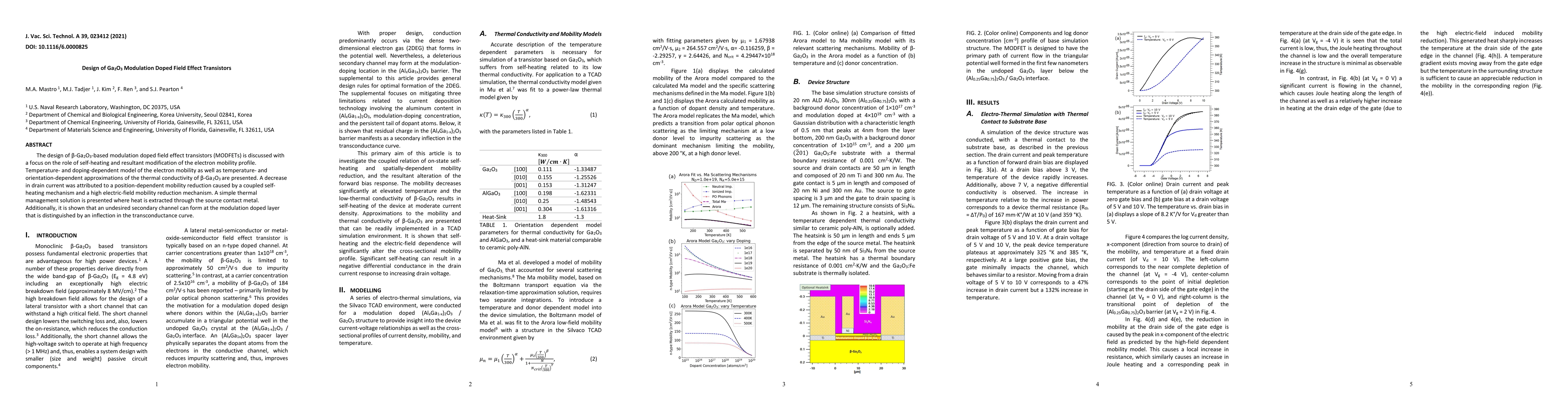
The design of beta-Ga2O3-based modulation doped field effect transistors (MODFETs) is discussed with a focus on the role of self-heating and resultant modification of the electron mobility profile. Temperature- and doping-dependent model of the electron mobility as well as temperature- and orientation-dependent approximations of the thermal conductivity of beta-Ga2O3 are presented. A decrease in drain current was attributed to a position-dependent mobility reduction caused by a coupled self-heating mechanism and a high electric-field mobility reduction mechanism. A simple thermal management solution is presented where heat is extracted through the source contact metal. Additionally, it is shown that an undesired secondary channel can form at the modulation doped layer that is distinguished by an inflection in the transconductance curve.

Citation & Reference Network Visualization

This graph shows how this paper is connected to other research. The current paper is shown in dark gray, papers that cite it are in green, and papers it references are in blue. You can:

Current Paper
Papers citing this work (Citations)
Papers cited by this work (References)

• Hover over any node to see the paper title

• Click a node to view that paper's details

• Drag nodes to rearrange the graph

• Use the zoom controls (bottom right) to zoom in/out

Citations and References

Title Authors Year Actions
Investigating Viability of Split-Stepped Gate Field Plate Design on Ga2O3 MOSFET for High Power Applications
Priyanshi Goyal, H. Kaur
2024
View Paper
High quality β-Ga2O3 bulk crystals, grown by edge-defined film-fed growth method: Growth features, structural, and thermal properties
D. Bauman, Dmitrii Iu. Panov, V. Spiridonov, A. Kremleva, A. Asach, E. Tambulatova, A. V. Sakharov, A. Romanov
2023
View Paper
Performance and stability of Al-doped HfGaO thin-film transistors deposited by vapor cooling condensation system
H. Lee, G. Zhu, Ching-Ting Lee
2023
View Paper
Design and simulation of T‐gate AlN/β‐Ga2O3 HEMT for DC, RF and high‐power nanoelectronics switching applications
Rajan Singh, G. Rao, T. Lenka, S. Prasad, N. Boukortt, G. Crupi, H. Nguyen
2023
View Paper
Critical review of Ohmic and Schottky contacts to β-Ga2O3
Luke A. M. Lyle
2022
View Paper
A Comprehensive Review on Recent Developments in Ohmic and Schottky Contacts on Ga2O3 for Device Applications
Hardhyan Sheoran, Vikram Kumar, Rajendra Singh
2022
View Paper
Design of microwave β-(Al x Ga 1− x )2O3/Ga2O3 lateral Schottky barrier diodes
Dudekula Shaikshavali, D. Kannadassan
2022
View Paper
Two inch diameter, highly conducting bulk β-Ga2O3 single crystals grown by the Czochralski method
Z. Galazka, S. Ganschow, Palvan Seyidov, K. Irmscher, Mike Pietsch, T. Chou, S. Bin Anooz, Raimund Grueneberg, A. Popp, A. Dittmar, A. Kwasniewski, Manuela Suendermann, D. Klimm, T. Straubinger, T. Schroeder, M. Bickermann
2022
View Paper

Comments (0)

This website uses cookies to ensure you get the best experience. Learn more