Publication
Metrics
AI Quick Summary
Researchers designed a Time-Domain Converter (TDC) ASIC with temperature compensation using TSMC 180nm process technology, achieving time resolutions of up to 73ps under various temperatures.
Paper Preview
Abstract
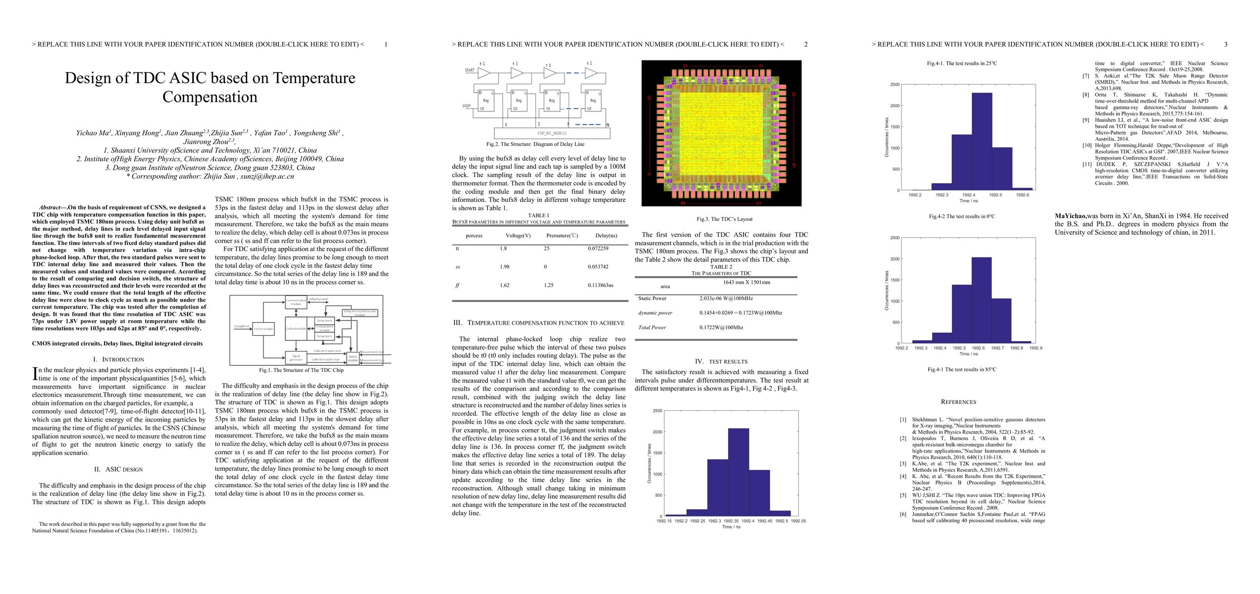
.On the basis of requirement of CSNS, we designed a TDC chip with temperature compensation function in this paper, which employed TSMC 180nm process. Using delay unit bufx8 as the major method, delay lines in each level delayed input signal line through the bufx8 unit to realize fundamental measurement function. The time intervals of two fixed delay standard pulses did not change with temperature variation via intra-chip phase-locked loop. After that, the two standard pulses were sent to TDC internal delay line and measured their values. Then the measured values and standard values were compared. According to the result of comparing and decision switch, the structure of delay lines was reconstructed and their levels were recorded at the same time. We could ensure that the total length of the effective delay line were close to clock cycle as much as possible under the current temperature. The chip was tested after the completion of design. It was found that the time resolution of TDC ASIC was 73ps under 1.8V power supply at room temperature while the time resolutions were 103ps and 62ps at 85$^\circ$ and 0$^\circ$, respectively.
AI Key Findings
Get AI-generated insights about this paper's methodology, results, significance, and more — seven facets brought into focus.
Impact
Paper Details
PDF Preview
Key Terms
Citation Network
Current paper (gray), citations (green), references (blue)
Display is limited for performance on very large graphs.
Discussion 0