Designing low-cost TaC virtual substrates for $Al_xGa_{1-x}N$ epitaxy
Publication
Metrics
AI Quick Summary
This paper identifies TaC as a low-cost, lattice-matched substrate for growing high-quality $Al_xGa_{1-x}N$ epitaxial layers, demonstrating improved film quality through optimized sputtering and annealing processes. The study highlights the potential for TaC substrates to enable advanced optoelectronic and power electronic applications.
Paper Preview
Abstract
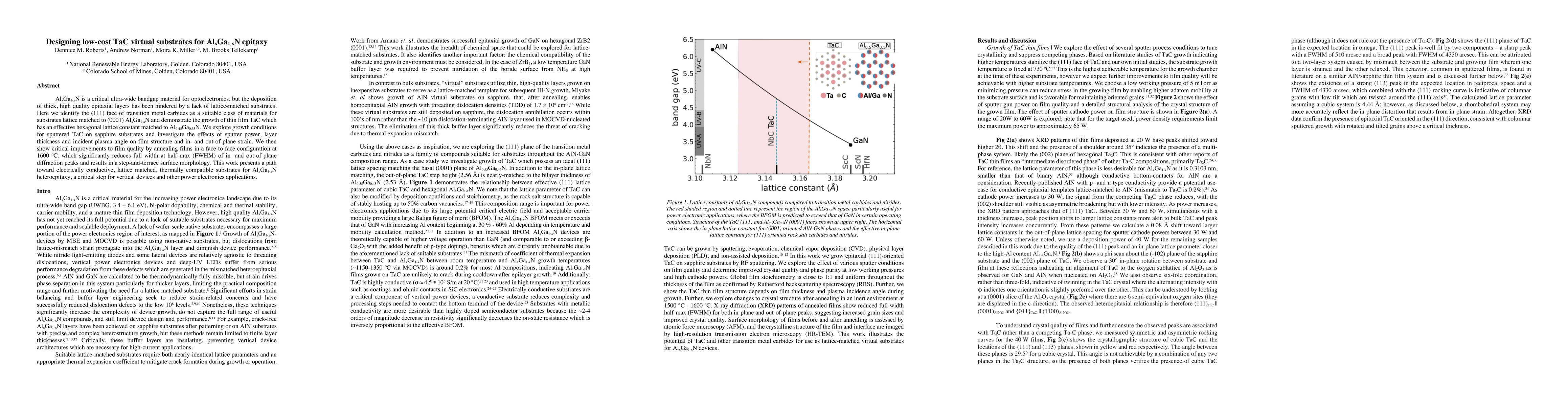
$Al_xGa_{1-x}N$ is a critical ultra-wide bandgap material for optoelectronics, but the deposition of thick, high quality epitaxial layers has been hindered by a lack of lattice-matched substrates. Here we identify the (111) face of transition metal carbides as a suitable class of materials for substrates lattice matched to (0001) $Al_xGa_{1-x}N$ and demonstrate the growth of thin film TaC which has an effective hexagonal lattice constant matched to $Al_{0.45}Ga_{0.55}N$. We explore growth conditions for sputtered TaC on sapphire substrates and investigate the effects of sputter power, layer thickness and incident plasma angle on film structure and in- and out-of-plane strain. We then show critical improvements to film quality by annealing films in a face-to-face configuration at 1600 $^\circ$C, which significantly reduces full width at half max (FWHM) of in- and out-of-plane diffraction peaks and results in a step-and-terrace surface morphology. This work presents a path toward electrically conductive, lattice matched, thermally compatible substrates for $Al_xGa_{1-x}N$ heteroepitaxy, a critical step for vertical devices and other power electronics applications.
AI Key Findings
Get AI-generated insights about this paper's methodology, results, significance, and more — seven facets brought into focus.
Impact
Paper Details
Authors
PDF Preview
Key Terms
Citation Network
Current paper (gray), citations (green), references (blue)
Display is limited for performance on very large graphs.
Discussion 0