Deterministic Thermal Sculpting of Large-Scale 2D Semiconductor Nanocircuits
Publication
Metrics
AI Quick Summary
This paper presents a method for deterministically engineering large-scale 2D semiconductor nanocircuits using thermal Sculpting and Scanning Probe Lithography. It demonstrates the fabrication of few-layer MoS2 nanostructures with high-resolution local conductivity maps, showcasing their potential for scalable integration in ultra-compact electronic devices.
Paper Preview
Abstract
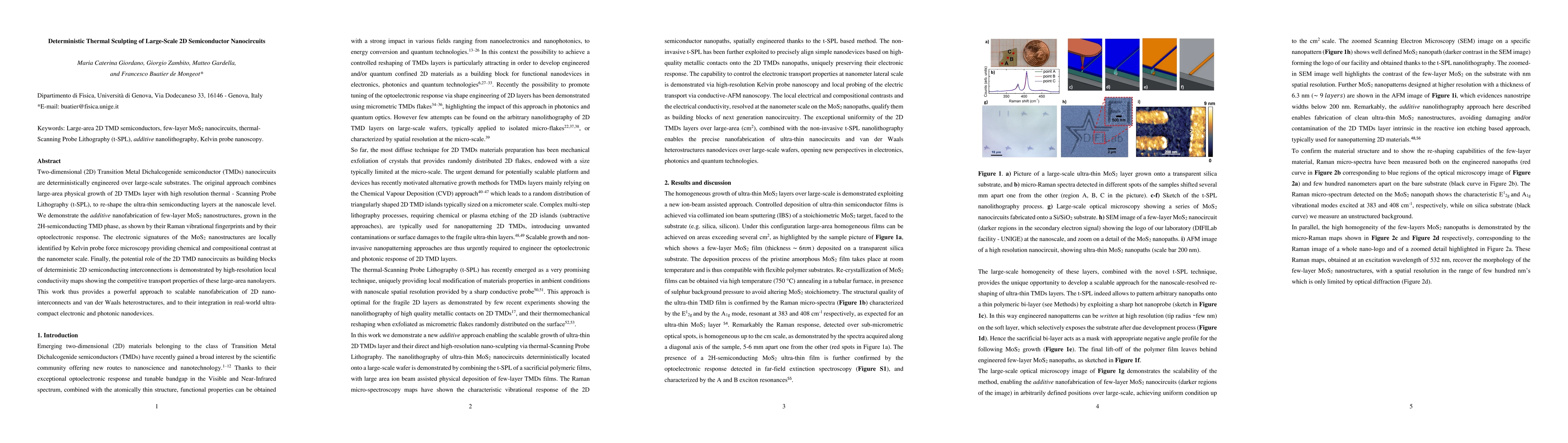
Two-dimensional (2D) Transition Metal Dichalcogenide semiconductor (TMDs) nanocircuits are deterministically engineered over large-scale substrates. The original approach combines large-area physical growth of 2D TMDs layer with high resolution thermal - Scanning Probe Lithography (t-SPL), to reshape the ultra-thin semiconducting layers at the nanoscale level. We demonstrate the additive nanofabrication of few-layer MoS2 nanostructures, grown in the 2H-semiconducting TMD phase, as shown by their Raman vibrational fingerprints and by their optoelectronic response. The electronic signatures of the MoS2 nanostructures are locally identified by Kelvin probe force microscopy providing chemical and compositional contrast at the nanometer scale. Finally, the potential role of the 2D TMD nanocircuits as building blocks of deterministic 2D semiconducting interconnections is demonstrated by high-resolution local conductivity maps showing the competitive transport properties of these large-area nanolayers. This work thus provides a powerful approach to scalable nanofabrication of 2D nano-interconnects and van der Waals heterostructures, and to their integration in real-world ultra-compact electronic and photonic nanodevices.
AI Key Findings
Get AI-generated insights about this paper's methodology, results, significance, and more — seven facets brought into focus.
Impact
Paper Details
Authors
PDF Preview
Key Terms
Citation Network
Current paper (gray), citations (green), references (blue)
Display is limited for performance on very large graphs.
Discussion 0