The research methodology involved fabricating a test element group (TEG) of linear APD on a Silicon on Insulator (SOI) process, simulating electric field distribution, and measuring current-voltage (IV) characteristics to examine the avalanche mechanism.
Development of the Pixelated Photon Detector Using Silicon on Insulator Technology for TOF-PET
Publication
Metrics
AI Quick Summary
Researchers developed a new pixelated photon detector using Silicon on Insulator technology to improve sensitivity and response speed in Time-Of-Flight Positron Emission Tomography (TOF-PET). The design incorporates a linear avalanche integration detector with an avalanche photodiode for reduced dark count noise and dead time.
Quick Answers
What is "Development of the Pixelated Photon Detector Using Silicon on Insulator Technology for TOF-PET" about?
Researchers developed a new pixelated photon detector using Silicon on Insulator technology to improve sensitivity and response speed in Time-Of-Flight Positron Emission Tomography (TOF-PET). The design incorporates a linear avalanche integration detector with an avalanche photodiode for reduced dark count noise and dead time.
What methodology did the authors use?
The research methodology involved fabricating a test element group (TEG) of linear APD on a Silicon on Insulator (SOI) process, simulating electric field distribution, and measuring current-voltage (IV) characteristics to examine the avalanche mechanism. More in Methodology →
What are the key results?
Simulation results showed that the Non Deep N-Well type had a thinner depletion area and more controlled electric field distribution at the P+ edge. — Measurement results indicated that guard ring structure increased breakdown voltage, suggesting it effectively controls electric field concentration at the P+ edge. More in Key Results →
Why is this work significant?
This research is important for improving the positional resolution of scintillation detectors by measuring light emission patterns in scintillators with higher sensitivity and faster response. The proposed Pixelated Linear Avalanche Integration Detector (SOI-Plaid) using Silicon on Insulator technology offers high-speed, low-noise signal reading with smaller gain of linear APD, overcoming limitations of conventional SPADs. More in Significance →
What are the main limitations?
The study focused on inspecting only four structures, which might not fully represent the overall performance of the SOI-APD. — The measurement results showed limited avalanche multiplication effect, suggesting further optimization is needed for enhanced photon detection efficiency. More in Limitations →
Abstract
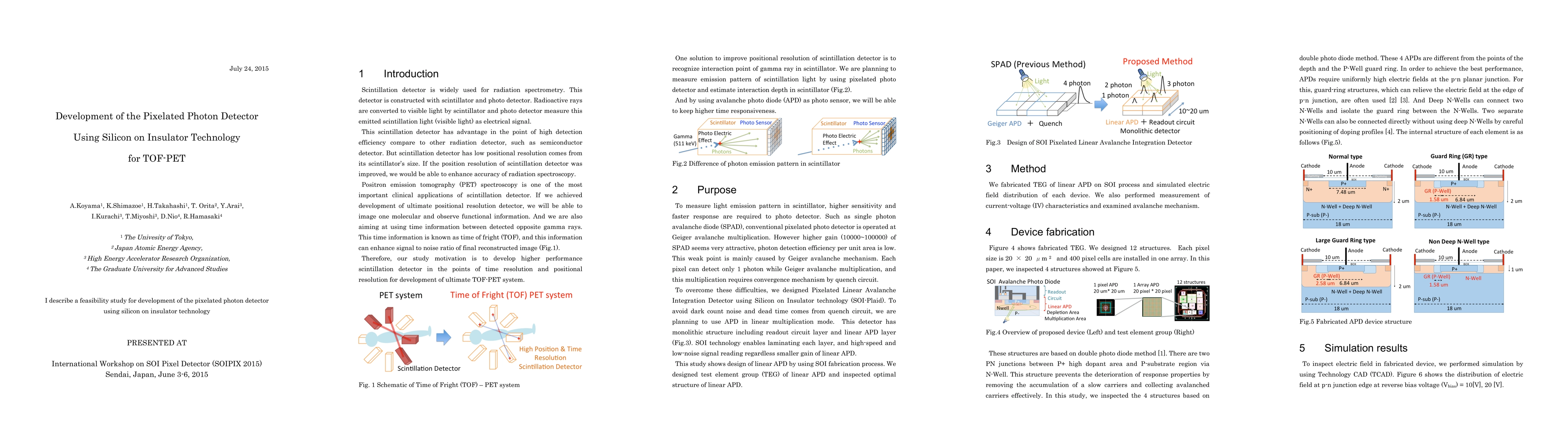
To measure light emission pattern in scintillator, higher sensitivity and faster response are required to photo detector. Such as single photon avalanche diode (SPAD), conventional pixelated photo detector is operated at Geiger avalanche multiplication. However higher gain of SPAD seems very attractive, photon detection efficiency per unit area is low. This weak point is mainly caused by Geiger avalanche mechanism. To overcome these difficulties, we designed Pixelated Linear Avalanche Integration Detector using Silicon on Insulator technology (SOI-Plaid). To avoid dark count noise and dead time comes from quench circuit, we are planning to use APD in linear multiplication mode. SOI technology enables laminating readout circuit and APD layer, and high-speed and low-noise signal reading regardless smaller gain of linear APD. This study shows design of linear APD by using SOI fabrication process. We designed test element group (TEG) of linear APD and inspected optimal structure of linear APD.
Key Findings, in focus
Seven facets of this paper, analysed and brought into focus by AI.
This research is important for improving the positional resolution of scintillation detectors by measuring light emission patterns in scintillators with higher sensitivity and faster response.
- Simulation results showed that the Non Deep N-Well type had a thinner depletion area and more controlled electric field distribution at the P+ edge.
- Measurement results indicated that guard ring structure increased breakdown voltage, suggesting it effectively controls electric field concentration at the P+ edge.
- Non Deep N-Well type demonstrated the highest breakdown voltage, indicating a more gradual electric field increase in a narrow region with bias voltage.
This research is important for improving the positional resolution of scintillation detectors by measuring light emission patterns in scintillators with higher sensitivity and faster response. The proposed Pixelated Linear Avalanche Integration Detector (SOI-Plaid) using Silicon on Insulator technology offers high-speed, low-noise signal reading with smaller gain of linear APD, overcoming limitations of conventional SPADs.
The development of a Pixelated Linear Avalanche Integration Detector using Silicon on Insulator technology (SOI-Plaid) for Time-of-Flight Positron Emission Tomography (TOF-PET) applications, which offers improved speed, lower noise, and better control over electric field distribution compared to conventional SPADs.
This work introduces a novel approach to overcome the limitations of SPADs by utilizing Avalanche Photodiodes (APDs) in linear multiplication mode with Silicon on Insulator technology, resulting in a monolithic structure that integrates readout circuits and APD layers for enhanced performance in scintillation detectors.
- The study focused on inspecting only four structures, which might not fully represent the overall performance of the SOI-APD.
- The measurement results showed limited avalanche multiplication effect, suggesting further optimization is needed for enhanced photon detection efficiency.
- Expand the investigation to more diverse APD structures to validate the findings and improve overall performance.
- Explore additional techniques to enhance avalanche multiplication and photon detection efficiency in the proposed SOI-APD design.
Impact
Paper Details
PDF Preview
Key Terms
Citation Network
Current paper (gray), citations (green), references (blue)
Display is limited for performance on very large graphs.
Discussion 0