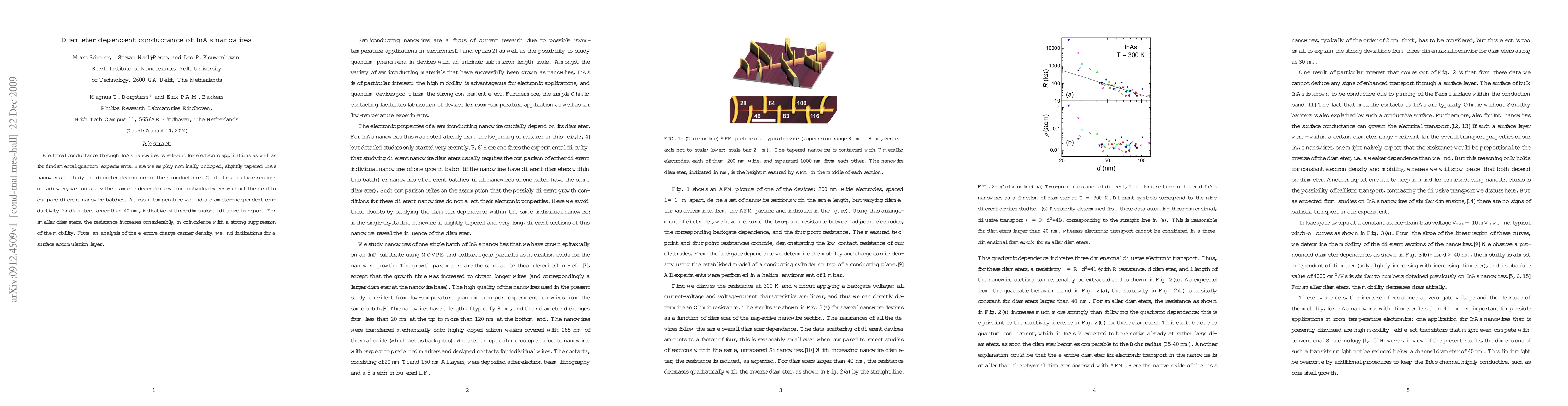
ArxivLens

Quick Summary:

This study investigates the diameter-dependent conductance of InAs nanowires, finding that larger diameters (over 40 nm) exhibit diameter-independent conductivity due to three-dimensional transport. For smaller diameters, resistance increases significantly, accompanied by reduced mobility and evidence of a surface accumulation layer.

Journal Reference: J. Appl. Phys. 106, 124303 (2009)
DOI: 10.1063/1.3270259
arXiv Id: 0912.4509
Comments: 9 pages, 5 figures
Date Published: 2009-12-23
Date Updated: 2009-12-23

Categories:

Key Terms (TF-IDF):

diameter (0.327)
nanowires (0.307)
conductance (0.267)
dependence (0.186)
nanowire (0.182)
wire (0.182)
diffusive (0.170)
room temperature (0.170)
room (0.164)
resistance (0.159)
carrier (0.158)
electrical (0.156)
mobility (0.152)
suppression (0.151)
considerably (0.151)
slightly (0.151)
conductivity (0.150)
nm (0.145)
sections (0.143)
employ (0.133)
License: http://arxiv.org/licenses/nonexclusive-distrib/1.0/

Summary:

Electrical conductance through InAs nanowires is relevant for electronic applications as well as for fundamental quantum experiments. Here we employ nominally undoped, slightly tapered InAs nanowires to study the diameter dependence of their conductance. Contacting multiple sections of each wire, we can study the diameter dependence within individual wires without the need to compare different nanowire batches. At room temperature we find a diameter-independent conductivity for diameters larger than 40 nm, indicative of three-dimensional diffusive transport. For smaller diameters, the resistance increases considerably, in coincidence with a strong suppression of the mobility. From an analysis of the effective charge carrier density, we find indications for a surface accumulation layer.

Citation & Reference Network Visualization

This graph shows how this paper is connected to other research. The current paper is shown in dark gray, papers that cite it are in green, and papers it references are in blue. You can:

Current Paper
Papers citing this work (Citations)
Papers cited by this work (References)

• Hover over any node to see the paper title

• Click a node to view that paper's details

• Drag nodes to rearrange the graph

• Use the zoom controls (bottom right) to zoom in/out

Citations and References

Title Authors Year Actions
Electronic Transport and Quantum Phenomena in Nanowires
G. Badawy, E. Bakkers
2024
View Paper
Diameter Control of GaSb Nanowires Revealed by In Situ Environmental Transmission Electron Microscopy
M. Marnauza, Robin Sjökvist, S. Lehmann, K. Dick
2023
View Paper
Automated Computer Vision-Enabled Manufacturing of Nanowire Devices
T. Potočnik, Peter J. Christopher, R. Mouthaan, T. Albrow-Owen, Oliver J. Burton, C. Jagadish, H. Tan, T. Wilkinson, S. Hofmann, H. Joyce, J. Alexander-Webber
2022
View Paper
Large-Composition-Range Pure-Phase Homogeneous InAs1-xSbx Nanowires.
Lianjun Wen, D. Pan, Lei Liu, S. Tong, Ran Zhuo, Jianhua Zhao
2021
View Paper
Effect of Flow Rate Scaling on SAE-InAs Crystal Phase and Integration of Self-Catalyzed InAs/InSb Heterostructure Nanowires on Si (111) Substrate by MOCVD
D. Anandan, H. Yu, Ching-Ting Lee, C. Dee, A. A. Hamzah, E. Chang
2021
View Paper
A theoretical and experimental study on effect of growth time on self-catalyzed InAs nanowires
Xiaoye Wang, Xue Bai, Xiaoguang Yang, Xiaomin Liu, W. Du, Tao Yang
2020
View Paper
The transport properties of InAs nanowires: an introduction to MnAs/InAs heterojunction nanowires for spintronics
P. Uredat, M. T. Elm, R. Horiguchi, P. Klar, S. Hara
2020
View Paper
Nanowires for thermoelectric energy conversion
D. Vakulov
2020
View Paper
Anomalous Angle-Dependent Magnetotransport Properties of Single InAs Nanowires.
P. Uredat, Ryutaro Kodaira, R. Horiguchi, S. Hara, A. Beyer, K. Volz, P. Klar, M. T. Elm
2019
View Paper
Quantum‐Confinement‐Enhanced Thermoelectric Properties in Modulation‐Doped GaAs–AlGaAs Core–Shell Nanowires
S. Fust, Anton Faustmann, D. J. Carrad, J. Bissinger, B. Loitsch, M. Döblinger, J. Becker, G. Abstreiter, J. Finley, G. Koblmüller
2019
View Paper
Charge Transport in Hexagonal-Phase Core Silicon Nanowires
Marc Collette
2019
View Paper
A New Analytic Formula for Minority Carrier Decay Length Extraction from Scanning Photocurrent Profiles in Ohmic-Contact Nanowire Devices
C. Chu, M.-H. Mao, Che-Wei Yang, Hao-Hsiung Lin
2019
View Paper
Regaining a Spatial Dimension: Mechanically Transferrable Two-Dimensional InAs Nanofins Grown by Selective Area Epitaxy.
J. Seidl, J. G. Gluschke, Xiaoming Yuan, Xiaoming Yuan, S. Naureen, N. Shahid, H. Tan, C. Jagadish, A. Micolich, P. Caroff, P. Caroff
2019
View Paper
Visualization and investigation of the non-thermalized electrons in an InAs nanowire by scanning gate microscopy
A. Zhukov, C. Volk, A. Winden, H. Hardtdegen, T. Schäpers
2019
View Paper
Sn Incorporation in Ultrathin InAs Nanowires for Next-Generation Transistors Characterized by Atom Probe Tomography
A. D. Giddings, P. Ramvall, T. Vasen, A. Afzalian, R. Hwang, Y. Yeo, M. Passlack
2019
View Paper
Electrical Properties of Indium Arsenide Nanowires and Their Field-Effect Transistors
M. Fu
2018
View Paper
Carrier concentration dependent photoluminescence properties of Si-doped InAs nanowires
M. Sonner, J. Treu, K. Saller, H. Riedl, J. Finley, G. Koblmüller
2018
View Paper
Surface State Dynamics Dictating Transport in InAs Nanowires.
D. Lynall, S. Nair, David Gutstein, A. Shik, I. Savelyev, M. Blumin, H. Ruda
2018
View Paper
Stability of charged density waves in InAs nanowires in an external magnetic field
A. Zhukov, C. Volk, A. Winden, H. Hardtdegen, T. Schäpers
2017
View Paper
Facile growth of density- and diameter-controlled GaN nanobridges and their photodetector application
Jin-Ho Kang, Muhammad Ali Johar, B. Alshehri, E. Dogheche, S. Ryu
2017
View Paper
Size dependent properties of one dimensional CdSe micro/nanostructures
Chetna Narula, R. Chauhan
2017
View Paper
Shiba Bound States across the Mobility Edge in Doped InAs Nanowires.
A. Assouline, C. Feuillet-Palma, A. Zimmers, H. Aubin, M. Aprili, J. Harmand
2017
View Paper
Contacting of Si/SiO2 core/shell nanowires using laser photolithography
F. Benyettou, A. Aissat, M. Benamar, I. Berbezier
2017
View Paper
Features of electron gas in InAs nanowires imposed by interplay between nanowire geometry, doping and surface states
V. Degtyarev, S. Khazanova, N. Demarina
2017
View Paper
Two-probe atomic-force microscope manipulator and its applications.
A. Zhukov, Vasily S. Stolyarov, Vasily S. Stolyarov, O. V. Kononenko, O. V. Kononenko
2017
View Paper
Roughness scattering induced insulator-metal-insulator transition in a quantum wire
H. Fu, M. Sammon, B. Shklovskii
2017
View Paper
Effect of nanohole size on selective area growth of InAs nanowire arrays on Si substrates
Xiaoye Wang, Wenyuan Yang, Baojun Wang, X. Ji, Shengyong Xu, Wen Wang, Qing Chen, Tao Yang
2017
View Paper
Impact of doping and diameter on the electrical properties of GaSb nanowires
Aein S Babadi, J. Svensson, E. Lind, L. Wernersson
2017
View Paper
Diameter-driven crossover in resistive behaviour of heavily doped self-seeded germanium nanowires
Stephen Connaughton, Maria Koleśnik‐Gray, R. Hobbs, O. Lotty, J. Holmes, V. Krstić
2016
View Paper
Direct Measurements of Fermi Level Pinning at the Surface of Intrinsically n-Type InGaAs Nanowires.
M. Speckbacher, J. Treu, T. J. Whittles, W. Linhart, Xiaomo Xu, K. Saller, V. Dhanak, G. Abstreiter, J. Finley, T. Veal, G. Koblmüller
2016
View Paper
In situ TEM electrical measurements of semiconductor and metal nanowires
M. Neklyudova
2016
View Paper
Conductance Quantization at Zero Magnetic Field in InSb Nanowires.
J. Kammhuber, M. Cassidy, Hao Zhang, Ö. Gül, F. Pei, Michiel W. A. de Moor, B. Nijholt, Kenji Watanabe, T. Taniguchi, D. Car, S. Plissard, E. Bakkers, L. Kouwenhoven
2016
View Paper
Orientation Dependence of Electromechanical Characteristics of Defect-free InAs Nanowires.
K. Zheng, Zhi Zhang, Yibin Hu, Pingping Chen, W. Lu, J. Drennan, Xiaodong Han, J. Zou
2016
View Paper
Doping evaluation of InP nanowires for tandem junction solar cells
Fredrik Lindelow, M. Heurlin, G. Otnes, Vilgailė Dagytė, D. Lindgren, O. Hultin, K. Storm, L. Samuelson, M. Borgström
2016
View Paper
Raman spectroscopy and electrical properties of InAs nanowires with local oxidation enabled by substrate micro-trenches and laser irradiation
Rawa Tanta, Morten Hannibal Madsen, Zhiyu Liao, P. Krogstrup, Tom Vosch, J. Nygård, T. Jespersen
2015
View Paper
Resolving ambiguities in nanowire field-effect transistor characterization.
S. Heedt, Isabel Otto, K. Sladek, H. Hardtdegen, J. Schubert, N. Demarina, H. Lüth, D. Grützmacher, T. Schäpers
2015
View Paper
Controlling the diameter distribution and density of InAs nanowires grown by Au-assisted methods
U. Gomes, D. Ercolani, V. Zannier, F. Beltram, L. Sorba
2015
View Paper
Diameter dependence of the thermal conductivity of InAs nanowires
M. Swinkels, M. V. Delft, D. S. Oliveira, A. Cavalli, I. Zardo, R. W. Heijden, E. Bakkers, E. Bakkers
2015
View Paper
Correlations of the mutual positions of the nodes of charge density waves in side-by-side placed InAs wires measured with scanning gate microscopy
A. Zhukov, C. Volk, A. Winden, H. Hardtdegen, T. Schäpers
2015
View Paper
Electrical and Surface Properties of InAs/InSb Nanowires Cleaned by Atomic Hydrogen.
J. Webb, J. Knutsson, M. Hjort, Sepideh Gorji Ghalamestani, K. Dick, R. Timm, A. Mikkelsen
2015
View Paper
Current-Voltage Characterization of Gallium Arsenide Nanowires Using a Conductive Atomic Force Microscopy
R. Muhammad, Y. Wahab, Z. Othaman, S. Sakrani
2015
View Paper
Contact properties of field-effect transistors based on indium arsenide nanowires thinner than 16 nm
T. Shi, M. Fu, D. Pan, Yao Guo, Jianhua Zhao, Qing Chen
2015
View Paper
In situ electrical characterization of tapered InAs nanowires in a transmission electron microscope with ohmic contacts
Chao Zhang, M. Neklyudova, L. Fang, Qiang Xu, Hui Wang, F. Tichelaar, H. Zandbergen
2015
View Paper
Electrical characteristics of field-effect transistors based on indium arsenide nanowire thinner than 10 nm
M. Fu, D. Pan, Y. Yang, T. Shi, Zhiyong Zhang, Jianhua Zhao, Hongqi Xu, Qing Chen
2014
View Paper
Investigations of local electronic transport in InAs nanowires by scanning gate microscopy at liquid helium temperatures
A. Zhukov, C. Volk, A. Winden, H. Hardtdegen, T. Schäpers
2014
View Paper
Quantum dots in InAs nanowires induced by surface potential fluctuations
K. Weis, S. Wirths, A. Winden, K. Sladek, H. Hardtdegen, H. Lüth, D. Grützmacher, T. Schäpers
2014
View Paper
Mobility enhancement by Sb-mediated minimisation of stacking fault density in InAs nanowires grown on silicon.
M. J. L. Sourribes, I. Isakov, M. Panfilova, Huiyun Liu, P. Warburton
2014
View Paper
First-principles study of quantum confinement and surface effects on the electronic properties of InAs nanowires
Feng Ning, Li-Ming Tang, Yong Zhang, Keqiu Chen
2013
View Paper
Influence of Dephasing and Geometrical Parameters on Quantum Correction to DC Conductance of Cylindrical Nanowires
B. J. Spisak, M. Wołoszyn, P. Wójcik
2013
View Paper
III–V nanowire photovoltaics: Review of design for high efficiency
R. LaPierre, A. Chia, S. Gibson, C. Haapamaki, J. Boulanger, R. Yee, P. Kuyanov, J. Zhang, N. Tajik, N. Jewell, K. K. A. Rahman
2013
View Paper
Current–Voltage Characterization of Individual As-Grown Nanowires Using a Scanning Tunneling Microscope
R. Timm, O. Persson, David L. J. Engberg, A. Fian, J. Webb, J. Wallentin, Andreas Jönsson, M. Borgström, L. Samuelson, A. Mikkelsen
2013
View Paper
Surface roughness induced electron mobility degradation in InAs nanowires
Fengyun Wang, Fengyun Wang, Senpo Yip, N. Han, K. Fok, Hao Lin, Jared J. Hou, Guofa Dong, T. Hung, Kwok Sum Chan, J. Ho
2013
View Paper
Band-offset effect on localization of carriers and p-type doping of InAs/GaAs core–shell nanowires
H. Shu, D. Cao, P. Liang, Xiaoshuang Chen, Wei Lu
2013
View Paper
Gate-induced transition between metal-type and thermally activated transport in self-catalyzed MBE-grown InAs nanowires
C. Blömers, T. Rieger, T. Grap, M. Raux, M. Lepsa, H. Lüth, D. Grützmacher, T. Schäpers
2013
View Paper
Inhomogeneous Si-doping of gold-seeded InAs nanowires grown by molecular beam epitaxy
C. Rolland, P. Caroff, C. Coinon, X. Wallart, R. Leturcq
2013
View Paper
Persistent enhancement of the carrier density in electron irradiated InAs nanowires
C. Durand, M. Berthe, Y. Makoudi, J. Nys, R. Leturcq, P. Caroff, B. Grandidier
2013
View Paper
Negative differential conductance in InAs wire based double quantum dot induced by a charged AFM tip
A. Zhukov, C. Volk, A. Winden, H. Hardtdegen, T. Schäpers
2012
View Paper
Non-linear direct-laser-write lithography for semiconductor nanowire characterisation
P. Parkinson, K. Peng, N. Jiang, Q. Gao, H. Tan, C. Jagadish
2012
View Paper
Comparison of gate geometries for tunable, local barriers in InAs nanowires
Peter D. Nissen, T. Jespersen, K. Grove‐Rasmussen, Attila Márton, Shivendra Upadhyay, M. Madsen, S. Csonka, J. Nygård
2012
View Paper
Direct-write non-linear photolithography for semiconductor nanowire characterization
Patrick Parkinson, N. Jiang, Qiang Gao, H. Tan, Chennupati Jagadish
2012
View Paper
Phase coherent transport in InSb nanowires
H. Yao, H. Günel, C. Blömers, K. Weis, J. Chi, J. Lu, Jie Liu, D. Grützmacher, T. Schäpers
2012
View Paper
Effect of Molecular Passivation on the Doping of InAs Nanowires
H. Shu, D. Cao, P. Liang, Shangzhong Jin, Xiaoshuang Chen, W. Lu
2012
View Paper
Electronic transport with dielectric confinement in degenerate InN nanowires.
C. Blömers, Jia Grace Lu, Liubing Huang, C. Witte, D. Grützmacher, H. Lüth, T. Schäpers
2012
View Paper
New method of creation of a rearrangeable local Coulomb potential profile and its application for investigations of local conductivity of InAs nanowires
A. Zhukov, C. Volk, A. Winden, H. Hardtdegen, T. Schäpers
2011
View Paper
Manipulating InAs nanowires with submicrometer precision.
Kilian Flöhr, M. Liebmann, K. Sladek, H. Günel, R. Frielinghaus, F. Haas, C. Meyer, H. Hardtdegen, T. Schäpers, D. Grützmacher, M. Morgenstern
2011
View Paper
Effect of Si-doping on InAs nanowire transport and morphology
S. Wirths, K. Weis, A. Winden, K. Sladek, C. Volk, S. Alagha, T. Weirich, M. Ahe, H. Hardtdegen, H. Lüth, N. Demarina, D. Grützmacher, T. Schäpers
2011
View Paper
Growth direction modulation and diameter-dependent mobility in InN nanowires
G. Koley, Z. Cai, E. Quddus, Jie Liu, M. Qazi, R. Webb
2011
View Paper
First-Principles Study of the Doping of InAs Nanowires: Role of Surface Dangling Bonds
H. Shu, Xiaoshuang Chen, Z. Ding, R. Dong, W. Lu
2011
View Paper
On the p-type character of Cd-and Zn-doped InAs nanowires
C. L. dos Santos, T. M. Schmidt, P. Piquini
2011
View Paper
Low-temperature conductance of the weak junction in InAs nanowire in the field of AFM scanning gate
A. Zhukov, C. Volk, A. Winden, H. Hardtdegen, T. Schäpers
2011
View Paper
The electrical and structural properties of n-type InAs nanowires grown from metal–organic precursors
C. Thelander, K. A. Dick, M. Borgström, L. Fröberg, P. Caroff, H. Nilsson, L. Samuelson
2010
View Paper
Influence of Different Growth Methods on the Electrical Properties of InAs Nanowires
M. Fu
2018
View Paper
Carrier trapping and activation at short-period wurtzite/zinc-blende stacking sequences in polytypic InAs nanowires
J. Becker, S. Morkötter, J. Treu, M. Sonner, M. Speckbacher, M. Döblinger, G. Abstreiter, J. Finley, G. Koblmüller
2018
View Paper
Development of new characterization techniques for III-V nanowire devices
O. Persson
2017
View Paper
Morphology control, electronic properties and evolution of light emission in faceted indium oxide structures
H. Ouacha, U. Kleineberg, H. Al-Brithen
2017
View Paper
III–V Nanowire Transistors for Low-Power Logic Applications: A Review and Outlook
Chen Zhang, Xiuling Li
2016
View Paper
Infuence of surface and crystal structure on the conductivity of individual InAs and InP nanowires
L. Kral
2015
View Paper
Tunable single hole regime of a silicon field effect transistor in standard CMOS technology
M. Turchetti, H. Homulle, F. Sebastiano, G. Ferrari, E. Charbon, E. Prati
2015
View Paper
Fabrication of Si and Ge vertical nanowire for transistor applications
C. Chu, Ming-Kun Huang, Gen-feng Wu, C. Chu, Shu‐Han Hsu, G. Luo
2015
View Paper
Intrinsische Quantenpunkte in InAs-Nanodrähten
K. Weis, Thomas Schäpers
2014
View Paper
Quantum transport in nanowire based hybrid devices
H. Günel, T. Schäpers
2013
View Paper

Comments (0)

This website uses cookies to ensure you get the best experience. Learn more